Introduction
Organic substrate PCBs open up a world of possibilities for electronic hobbyists eager to dive into custom PCB design and homebrew electronics. These boards use polymer-based materials that provide flexibility, affordability, and ease of fabrication right in your workshop. Whether you are crafting PCB art or building functional gadgets, organic substrates allow for creative experimentation without the rigidity of ceramic alternatives. Hobbyists appreciate how these materials support intricate traces and multilayer designs suitable for personal projects. This article explores practical ways to harness organic substrate PCB DIY techniques, sparking innovation in your electronics endeavors. Get ready to transform simple ideas into tangible creations.
What Are Organic Substrate PCBs and Why Do They Matter for Hobbyists
Organic substrate PCBs rely on materials like epoxy resins reinforced with glass fibers or other polymers to form the core insulating layer. These substrates conduct electricity through copper traces etched or milled onto their surface, enabling reliable signal paths in compact forms. Unlike inorganic options, organic substrates offer lower cost and simpler processing, making them ideal for PCB projects for hobbyists. They balance mechanical strength with thermal stability, supporting soldering and component mounting in home settings. Industry standards such as IPC-6012E define qualification criteria for these rigid boards, ensuring performance consistency even in DIY contexts.
The relevance for hobbyists lies in their versatility for custom PCB design. Organic substrates allow shaping boards into non-standard geometries, perfect for PCB art or wearable tech. They resist common workshop hazards like moderate heat and humidity better than uncoated alternatives. Factory insights reveal that these materials maintain dielectric integrity under typical operating voltages, vital for homebrew electronics. Their lightweight nature simplifies prototyping, reducing iteration time. Embracing organic substrate PCB DIY empowers creators to prototype rapidly and iterate designs freely.
Technical Principles Behind Organic Substrate PCBs
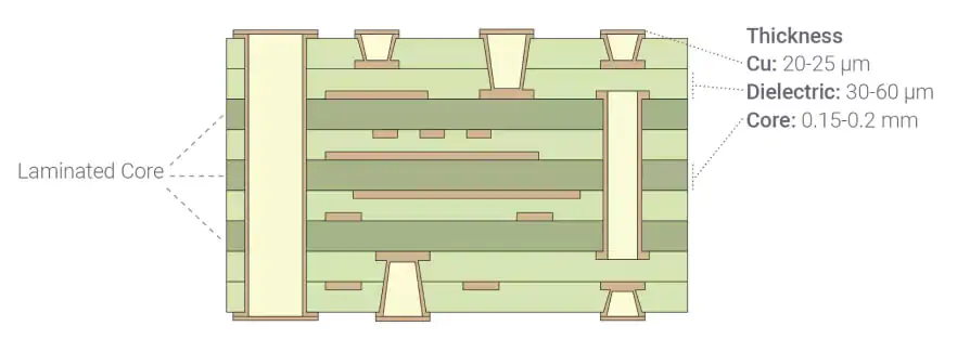
The foundation of organic substrate PCBs starts with the laminate structure, where resin binds reinforcing fibers to create a stable base. Copper foil bonds to this surface via heat and pressure, forming the conductive layer ready for patterning. Etching removes excess copper using chemical solutions, revealing the circuit design transferred from artwork. This process adheres to principles outlined in IPC-A-600K for board acceptability, focusing on trace width uniformity and surface finish. Hobbyists benefit from the material's low coefficient of thermal expansion, minimizing stress during soldering.
Multilayer organic substrates stack cores with prepregs, aligning vias for interlayer connections. Drilling and plating create conductive paths, essential for complex homebrew electronics. The organic matrix provides insulation with controlled permittivity, reducing signal crosstalk in dense layouts. Factory-driven testing verifies warpage limits, ensuring flatness for component placement. Understanding these mechanisms allows precise custom PCB design, avoiding common pitfalls like delamination from moisture exposure.
Dielectric properties influence high-frequency performance, though hobbyists often prioritize DC and low-speed applications. Organic substrates handle currents up to standard component ratings without excessive heating. Adhesion strength between copper and substrate prevents peeling under vibration, common in portable projects. These principles guide scalable fabrication from single boards to batches.
Practical DIY Projects Using Organic Substrate PCBs
Start with a luminous PCB art installation using organic substrate PCB DIY methods. Design fractal patterns in free software, print onto transparency, and transfer to copper-clad board via toner method. Etch with ferric chloride, then populate with addressable LEDs for dynamic displays. This project showcases PCB projects for hobbyists by blending aesthetics with functionality, creating wall art that pulses to music. Mount on wood for a rustic frame, highlighting the substrate's machinability.

Advance to a portable sensor node for environmental monitoring. Route traces for temperature, humidity sensors, and a microcontroller on a flexible organic variant like polyimide film. Mill the board with a CNC router for precise cutouts, enabling enclosure integration. Solder surface-mount parts, following J-STD-020E guidelines for moisture sensitivity to avoid reflow defects. This homebrew electronics build demonstrates data logging via wireless modules, deployable in gardens or workshops.
Craft wearable badges with embedded LEDs and buttons on thin organic substrates. Laser-cut shapes from laminate sheets, then pattern circuits using photoresist exposure. The material's bendability suits curved forms, ideal for convention swag or interactive jewelry. Program microcontrollers for light shows triggered by touch. Such PCB art projects foster community sharing among hobbyists.
Build a modular synthesizer voice using organic substrate PCBs. Dedicate boards to oscillators, filters, and mixers, with headers for stacking. Etch high-precision traces to minimize noise, using ground planes for shielding. This setup scales for larger instruments, embodying custom PCB design creativity. Experiment with component values for unique timbres.
Best Practices for Organic Substrate PCB DIY Fabrication
Select copper-clad laminates with 1 oz foil for most hobbyist needs, ensuring good etch uniformity. Prepare designs with 6 mil minimum trace spacing to prevent shorts, verifiable under magnification. Clean substrates thoroughly before transfer to avoid adhesion failures. Use gloves during etching to protect skin and maintain solution efficacy. Post-etch, neutralize residues with baking soda rinse for safe handling.
For multilayer attempts, align inner layers precisely using registration holes. Bake boards pre-soldering to drive out moisture, aligning with JEDEC practices. Employ flux pens for clean joints, inspecting for cold solder under light. Store unused substrates in dry conditions to preserve integrity. These steps mirror factory protocols, elevating homebrew electronics quality.
Test continuity with multimeters before powering up, tracing potential opens. Incorporate test points in designs for probing. Document iterations in notebooks, refining for future PCB projects for hobbyists. Safety first: ventilate etching areas and dispose chemicals responsibly.
Troubleshooting Common Challenges in Organic Substrate PCB DIY
Under-etched traces often stem from weak developer or short exposure, resolved by agitating baths evenly. Double-sided boards may misalign; use clamps during transfer. Warped substrates indicate improper storage; flatten under weights overnight. Solder bridges clear with wick and flux, avoiding excessive heat to prevent delamination.
Component overheating during soldering points to poor thermal relief; add pads in redesigns. Noisy signals suggest ground loop issues; implement pours next time. Faded toner lifts from dirty boards; acetone wipe beforehand helps. Persistent issues warrant standard checks like IPC criteria for defects.
Conclusion
Organic substrate PCB DIY fuels endless creativity in custom PCB design and PCB art. From glowing installations to sensor arrays, these projects empower electronic hobbyists to realize visions affordably. Adhering to best practices ensures reliable homebrew electronics outcomes. Experiment boldly, leveraging material flexibility for unique forms. Your workshop becomes a hub of innovation, blending art and engineering seamlessly.
FAQs
Q1: What materials work best for organic substrate PCB DIY projects?
A1: Organic substrates like epoxy-glass laminates suit most PCB projects for hobbyists due to their balance of strength and etchability. Select 1.6 mm thickness for stability in rigid designs. Flexible polyimides enable wearables. Always verify copper adhesion before patterning. These choices align with standard fabrication for durable results.
Q2: How do I start custom PCB design for homebrew electronics?
A2: Begin with schematic capture, then layout traces on organic substrate layers. Export Gerber files for verification. Prototype via toner transfer or milling for organic substrate PCB DIY. Test iteratively for functionality. This workflow streamlines PCB projects for hobbyists from concept to working board.
Q3: Can organic substrate PCBs handle PCB art applications?
A3: Yes, their machinability supports intricate shapes and colors via silkscreen. Etch artistic traces, add LEDs for illuminated effects. Flexible variants curve for sculptures. Maintain clearances per standards for reliability. PCB art thrives on these substrates' versatility in hobbyist creations.
Q4: What safety tips apply to organic substrate PCB DIY etching?
A4: Wear gloves, goggles, and ventilate to handle etchants safely. Neutralize wastes before disposal. Bake boards to expel moisture pre-assembly. Avoid inhaling fumes during soldering. These practices protect users in homebrew electronics sessions.
References
IPC-6012E — Qualification and Performance Specification for Rigid Printed Boards. IPC, 2017
IPC-A-600K — Acceptability of Printed Boards. IPC, 2020
J-STD-020E — Moisture/Reflow Sensitivity Classification. JEDEC, 2014


