Introduction
Magnetic Resonance Imaging (MRI) machines generate intense static magnetic fields, rapidly switching gradient fields, and high-power radiofrequency (RF) pulses to produce detailed images of the human body. Printed circuit boards (PCBs) within these systems control critical functions such as gradient amplifiers, RF transmitters, and receiver coils, making them vulnerable to electromagnetic interference (EMI) and essential for electromagnetic compatibility (EMC). Poor EMC in MRI PCB design can lead to image artifacts, system malfunctions, or safety hazards in the high-field environment typical of MRI rooms. Engineers must prioritize MRI PCB EMC design from the outset to mitigate radiated and conducted emissions while ensuring immunity to external disturbances. Regulatory compliance demands adherence to stringent standards, balancing performance with reliability in this demanding application. This article explores key strategies for MRI PCB EMI reduction, shielding techniques, grounding strategies, and testing protocols.
Why EMC/EMI Matters for MRI Machine PCBs
MRI systems operate at field strengths from 1.5T to 7T or higher, producing RF frequencies in the 64 MHz to 300 MHz range alongside gradient slew rates exceeding 200 T/m/s. These conditions create a harsh electromagnetic environment where PCB-generated noise can couple into sensitive receive chains, degrading signal-to-noise ratios and causing diagnostic errors. Conversely, external fields can induce voltages on PCB traces, leading to data corruption or component failure. Effective MRI PCB EMC design prevents both emissions and susceptibility, ensuring uninterrupted operation during scans that last minutes to hours. Compliance with medical EMC requirements also avoids costly redesigns and delays in certification processes. In summary, robust EMC practices safeguard patient safety and system uptime in clinical settings.

Key EMI Sources and EMC Challenges in MRI PCBs
EMI in MRI PCBs arises from multiple sources, including digital switching in microcontrollers, power supplies generating harmonics, and high-current gradient drivers with fast edges. Conductive coupling occurs via shared power/ground planes, while capacitive and inductive coupling affects nearby traces through fringing fields. Radiated emissions peak at clock harmonics and RF bands, potentially interfering with the MRI's Larmor frequency. MRI-specific challenges include susceptibility to the main B0 field, which induces eddy currents in conductive layers, and pulsed gradients causing mechanical vibrations that exacerbate noise. Multi-layer PCBs amplify these issues if layer transitions lack proper via stitching. Addressing these requires a holistic approach integrating layout, materials, and verification.
Fundamental Principles of MRI PCB EMC Design
EMC begins with PCB stackup selection, favoring multi-layer configurations with dedicated ground and power planes adjacent to signal layers to confine fields and provide low-impedance return paths. Stripline routing embeds sensitive traces between planes, minimizing radiation compared to microstrip on outer layers. Loop area reduction limits magnetic field generation per Ampere's law, achieved by short traces and parallel return paths. Component placement segregates noisy digital sections from analog RF paths, with guards around critical nodes. Material choices emphasize low-loss dielectrics to curb resonances, though MRI demands non-magnetic alloys for vias and enclosures. These principles form the foundation of MRI PCB EMC design, directly impacting emission spectra and immunity thresholds.
MRI PCB Shielding Techniques
Shielding confines EMI through conductive barriers that reflect or absorb waves, crucial for MRI where RF pulses demand >60 dB attenuation. PCB-level shielding employs metal cans or lids over oscillators and amplifiers, secured with multiple ground points for 360-degree contact. Via fencing along board edges, spaced at less than wavelength/20 of the highest frequency, creates a Faraday cage effect when stitched to inner planes. Edge plating connects outer copper pours to ground, enhancing containment. For MRI PCB shielding techniques, embedded metal layers or conductive coatings on sensitive areas block gradient-induced fields. Combining these with enclosure shielding ensures compliance, as unshielded traces can radiate into the bore. Engineers verify effectiveness through simulation before prototyping.
MRI PCB Grounding Strategies
Proper grounding minimizes potential differences that drive common-mode currents, starting with a single, unbroken reference plane spanning the entire board. Multi-point grounding connects all planes via dense via arrays, reducing inductance below 1 nH/cm for high frequencies. Star grounding suits low-frequency analog, but MRI PCB grounding strategies favor distributed planes for broadband performance, with stitching vias every 1/10 wavelength. Power islands tie to ground through decoupling capacitors forming low-pass filters. Chassis connections via capacitive coupling handle RF return paths without DC loops. Avoiding splits under traces prevents current detours that increase emissions. These strategies align with IPC-2221 guidelines for controlled impedance and noise suppression.
MRI PCB EMI Reduction Techniques
EMI reduction targets sources proactively, beginning with clock speeds minimized to essentials and spread-spectrum modulation to dilute peaks. Decoupling capacitors, placed within millimeters of IC pins, shunt high-frequency noise to ground with via-in-pad for minimal loop inductance. Ferrite beads and pi-filters at I/O ports attenuate conducted emissions above 30 MHz. Trace impedance matching to 50 ohms curbs reflections in RF sections. Differential routing for high-speed signals rejects common-mode noise. For MRI PCB EMI reduction, segregating partitions with guard traces grounded at both ends isolates domains. Layout symmetry ensures balanced returns, cutting differential-to-common-mode conversion.
EMC Testing for MRI PCBs
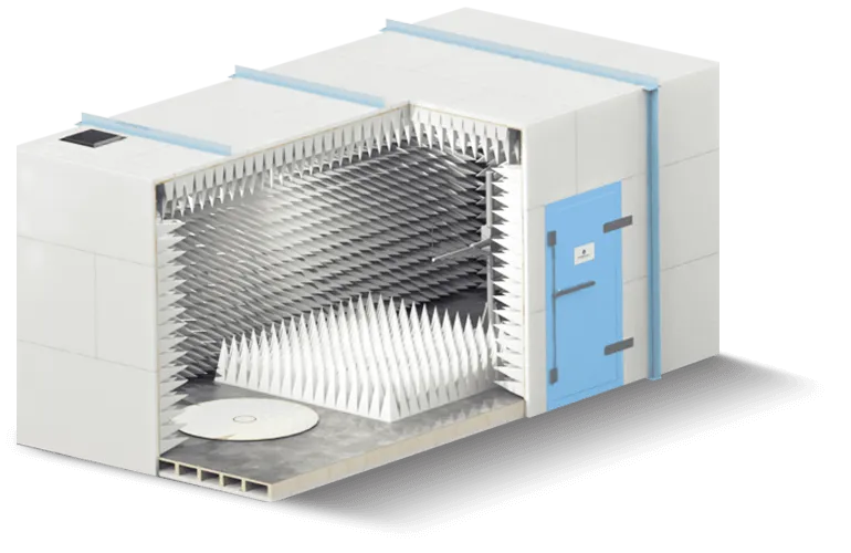
EMC testing verifies design under controlled disturbances, following IEC 60601-1-2 protocols for medical equipment. Radiated emissions measure fields from 150 kHz to 6 GHz in semi-anechoic chambers, targeting CISPR 11 Group 1 Class B limits. Immunity tests expose PCBs to 3 V/m RF fields, 8 kV ESD, and 100 V/m MRI-like pulses without performance loss. Conducted immunity applies surges up to 2 kV on power lines. Pre-compliance uses spectrum analyzers and LISNs for early detection. MRI-specific testing simulates gradient dB/dt up to 50 T/s. Iterative fixes post-test refine shielding and filtering until pass criteria meet essential performance definitions.
Best Practices for Regulatory Compliance in MRI PCBs
Integrate EMC from schematic capture, simulating fields with 3D solvers to predict hotspots. Prototype on production stackups, incorporating IPC-6012 qualification for reliability. Document risk analysis per ISO 14971, linking to EMC mitigations. Collaborate with test houses early for tailored setups. Firmware mitigations like error-correcting codes enhance robustness. These practices ensure MRI PCBs achieve certification, minimizing field failures.
Conclusion
MRI PCB EMC design demands meticulous attention to shielding techniques, grounding strategies, and EMI reduction to thrive in extreme fields. By leveraging solid planes, via stitching, and targeted filtering, engineers curb emissions and bolster immunity. EMC testing per established protocols confirms compliance, safeguarding diagnostic accuracy. Implementing these from concept to verification yields reliable, regulation-ready boards. Prioritizing these elements elevates MRI system performance and patient outcomes.
FAQs
Q1: What are essential MRI PCB shielding techniques for EMC compliance?
A1: MRI PCB shielding techniques include via fencing along edges, metal cans over noisy ICs, and edge plating to inner grounds. These create low-impedance barriers attenuating RF fields above 100 MHz. Combine with enclosure gaskets for full-system Faraday protection. Adhering to layer-adjacent planes enhances effectiveness, ensuring emissions stay below IEC limits.
Q2: How do MRI PCB grounding strategies reduce EMI?
A2: MRI PCB grounding strategies use continuous reference planes with dense stitching vias to minimize loop inductance and common-mode currents. Distributed multi-point connections suit broadband noise from gradients and RF. Avoid plane splits under traces to prevent high-emission detours. This setup provides return paths reducing radiated fields by over 20 dB in critical bands.
Q3: Why is EMC testing critical for MRI PCBs?
A3: EMC testing for MRI PCBs validates immunity to 10 V/m fields and emissions under CISPR 11, per IEC 60601-1-2. It simulates hospital EMI, including MRI pulses, ensuring no image degradation. Early pre-compliance cuts redesign costs. Passing confirms regulatory compliance for market approval.
Q4: What role does stackup play in MRI PCB EMI reduction?
A4: Stackup in MRI PCB EMI reduction features signal layers sandwiched between ground/power planes for field confinement. Six-layer builds with outer ground pours excel in high-density designs. Stripline routing cuts radiation versus microstrip. Optimized dielectric spacing controls impedance, suppressing harmonics.
References
IEC 60601-1-2 — Medical electrical equipment - Part 1-2: General requirements for basic safety and essential performance - Collateral standard: Electromagnetic compatibility - Requirements and tests. IEC, 2020
IPC-2221G — Generic Standard on Printed Board Design. IPC, 2017
IPC-6012E — Qualification and Performance Specification for Rigid Printed Boards. IPC, 2017


