Introduction
Printed circuit boards form the backbone of gaming consoles, enabling the high-performance computing required for immersive experiences in consumer electronics gaming consoles. These PCBs integrate processors, graphics units, memory modules, and connectivity interfaces into compact assemblies that handle demanding workloads like real-time rendering and multiplayer networking. Recent technological innovations have pushed PCB designs toward higher densities and faster signal speeds to support advanced features such as ray tracing and high-frame-rate outputs. As the gaming industry evolves, understanding these advancements is crucial for electrical engineers designing or procuring components. This article explores key innovations in gaming console PCBs, practical implementation strategies, and the future market outlook amid growing equipment gaming market demand for PCBs.
The Critical Role of PCBs in Gaming Consoles
Gaming console PCBs serve as the central interconnect platform, routing signals between high-speed digital components while managing power distribution and heat dissipation. In consumer electronics gaming consoles, these boards must accommodate multilayer stackups to separate signal, power, and ground planes, minimizing crosstalk and electromagnetic interference. The complexity arises from integrating ball grid array packages for CPUs and GPUs, which demand precise via-in-pad designs for reliable soldering. Electrical engineers prioritize signal integrity to maintain data rates exceeding 10 Gbps for features like 4K video output. Reliability under continuous operation also requires adherence to qualification standards such as IPC-6012E, ensuring performance specifications for rigid printed boards. Ultimately, these PCBs directly influence console responsiveness and longevity in competitive gaming environments.
Technological Innovations Driving PCB Performance
High-density interconnect (HDI) technology represents a major innovation in gaming console PCBs, utilizing microvias, blind vias, and buried vias to achieve finer line widths and spaces below 50 microns. This allows packing more components into smaller footprints, essential for compact handheld or next-generation stationary consoles supporting virtual reality peripherals. Advanced materials with low dielectric constants reduce signal propagation delays, enabling higher clock speeds for graphics processing units. Embedded passives and actives within the PCB layers further shrink overall volume while improving electrical performance. Thermal management innovations, such as metal-core substrates and embedded heat pipes, address heat from power-hungry processors. These developments ensure gaming console PCBs meet the demands of evolving graphics APIs and AI-accelerated rendering.
Engineers leverage sequential build-up processes in HDI fabrication to stack multiple microvia layers, enhancing routing density without compromising yield. Fine-pitch surface-mount components benefit from laser-drilled vias that align precisely with under-bump metallization. Signal equalization techniques integrated into the PCB layout compensate for losses at multi-gigabit frequencies. Power delivery networks employ decoupled capacitors strategically placed near IC loads to stabilize voltage rails. Compliance with IPC-6018D for high-density interconnect boards guides these designs, specifying qualification for microvia reliability.
High-Speed Signaling and Power Integrity Challenges
Gaming console PCBs face stringent requirements for high-speed differential pairs carrying PCIe, HDMI, and DDR memory signals, where impedance control is paramount to prevent reflections. Controlled impedance traces, often 100 ohms differential, demand precise layer thicknesses and material selection to match characteristic impedance. Return path optimization through dedicated ground planes reduces loop inductance, crucial for eye diagram integrity at data rates above 16 Gbps. Pre-emphasis and de-emphasis drivers in transceivers pair with PCB channel designs featuring back-drilling to eliminate stub effects. Electrical engineers simulate these channels using field solvers to predict insertion and return loss.
Power integrity analysis ensures stable supplies to mixed-signal circuits, mitigating simultaneous switching noise from multiple cores. Decoupling strategies include interplane capacitance formed by thin dielectrics between power and ground. Voltage regulator modules mounted directly on the PCB minimize trace drops. JEDEC J-STD-020E standards inform handling of moisture-sensitive devices during reflow, preventing delamination in multilayer assemblies. These practices sustain performance during prolonged gaming sessions with variable loads.
Thermal Management and Mechanical Reliability
Effective thermal dissipation in gaming console PCBs prevents throttling under sustained loads from integrated GPUs and CPUs generating over 200W. Vias filled with thermal grease or copper plating transfer heat to external heatsinks or vapor chambers. Material choices like high-Tg laminates maintain dimensional stability across reflow profiles up to 260°C. Warpage control during lamination follows IPC guidelines to avoid misalignment in high-layer counts. Finite element analysis predicts stress from coefficient of thermal expansion mismatches between copper and substrates.
Mechanical robustness supports drop tests and vibration in portable gaming devices, with edge plating and anchor vias reinforcing board edges. Solder joint reliability under thermal cycling relies on optimized pad geometries per J-STD specifications. These engineering approaches extend field life in consumer electronics gaming consoles.
Best Practices for Designing and Manufacturing Gaming Console PCBs
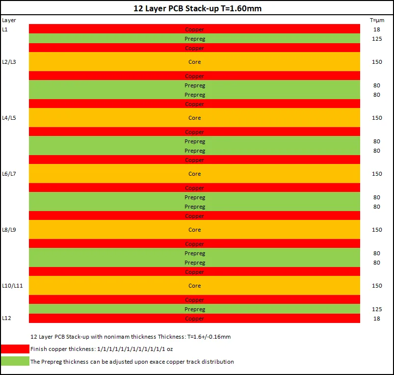
Start with a robust stackup planning that balances signal count, power delivery, and manufacturability, targeting 8 to 16 layers for mainstream designs. Simulate signal and power integrity early to iterate trace geometries before layout finalization. Select low-loss dielectrics like those with Dk under 3.5 for high-frequency sections. Incorporate test points and flying probes for in-circuit verification post-assembly. Fabrication partners should validate via chain integrity through electrical testing.
Assembly processes emphasize stencil design for fine-pitch BGAs, ensuring uniform solder paste volume. Reflow profiling per IPC-6012E minimizes defects like head-in-pillow. Incoming inspection of components verifies MSL ratings against JEDEC J-STD-020E. Functional testing under load replicates gaming workloads to catch early failures. Documentation of design rules supports scalability for future revisions.
Future Market Outlook and Emerging Trends
The equipment gaming market demand for PCBs continues to rise, driven by expansion in consumer electronics gaming consoles and hybrid PC-console ecosystems. Advancements in chiplet architectures will necessitate PCBs with support for optical interconnects and 2.5D packaging. Handheld and cloud-hybrid devices demand flexible-rigid hybrids for ergonomic forms. Sustainability pushes for lead-free processes and recyclable materials, aligning with ISO 14001 environmental standards. Integration of AI accelerators requires enhanced power planes and noise isolation.
By 2026, 8K resolutions and haptic feedback systems will elevate PCB complexity, with HDI Class 4 becoming standard. Market growth in emerging regions amplifies volume needs for cost-effective high-reliability boards. Engineers must anticipate these shifts to meet escalating performance benchmarks.
Conclusion
Gaming console PCBs embody cutting-edge engineering to deliver seamless high-fidelity experiences in consumer electronics gaming consoles. Innovations in HDI, high-speed materials, and thermal solutions address core challenges of density, speed, and reliability. Adhering to standards like IPC-6012E, IPC-6018D, and JEDEC J-STD-020E ensures manufacturability and performance. As equipment gaming market demand for PCBs surges, future designs will embrace chiplet integration and sustainable practices. Electrical engineers play a pivotal role in shaping this trajectory, optimizing for next-generation demands.
FAQs
Q1: What makes HDI technology essential for modern gaming console PCBs?
A1: HDI enables microvias and fine lines to fit more components in compact spaces, vital for consumer electronics gaming consoles with powerful GPUs and memory. It supports high-speed signals up to 25 Gbps while reducing board size. Manufacturing follows IPC-6018D for reliability. This density improves thermal efficiency and cuts material costs in high-volume production.
Q2: How do electrical engineers ensure signal integrity in gaming PCBs?
A2: Engineers control impedance with precise stackups and materials, using simulations to optimize trace lengths and vias. Back-drilling eliminates stubs for clean eye patterns at multi-Gbps rates. Ground planes provide low-inductance returns. Compliance with design rules prevents crosstalk in dense layouts for gaming equipment.
Q3: What drives the rising equipment gaming market demand for PCBs?
A3: Growing adoption of 4K/8K gaming, VR, and handhelds increases need for advanced multilayer and HDI PCBs. Convergence with PC architectures boosts performance requirements. Supply chain efficiencies support scaling production. Engineers focus on cost-performance balance amid this expansion.
Q4: What thermal strategies are best for high-power gaming console PCBs?
A4: Thermal vias, metal cores, and embedded heat spreaders dissipate heat from processors effectively. Low-CTE materials minimize warpage during operation. Simulations predict hotspots for heatsink placement. Standards like IPC-6012E guide qualification for long-term stability.
References
IPC-6012E — Qualification and Performance Specification for Rigid Printed Boards. IPC, 2017
IPC-6018D — Qualification and Performance Specification for High Density Interconnect (HDI) Printed Boards. IPC, 2020
JEDEC J-STD-020E — Moisture/Reflow Sensitivity Classification of Nonhermetic Solid State Surface Mount Devices. JEDEC, 2014


