Introduction
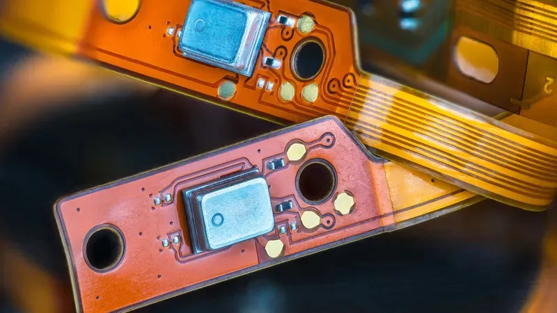
High-density interconnect (HDI) flexible PCBs represent a significant advancement in printed circuit board technology, enabling compact designs in demanding applications. These boards combine the flexibility of polyimide substrates with microvia structures to achieve higher component density and routing efficiency. Engineers increasingly rely on HDI flexible PCBs for devices where space constraints and mechanical flexibility are critical, such as wearables, medical implants, and aerospace systems. The integration of flexible PCB microvias and fine pitch traces allows for superior signal performance while maintaining bendability. This article explores the principles, manufacturing considerations, and best practices for implementing HDI flexible PCBs effectively.
What Are HDI Flexible PCBs and Why Do They Matter?
HDI flexible PCBs are multilayer flexible circuits that incorporate high-density features like blind, buried, and stacked microvias to connect inner layers without consuming surface real estate. Unlike traditional flexible PCBs, which rely on larger through-holes and wider traces, HDI versions use laser-drilled vias under 150 microns in diameter to support fine pitch components. This construction maximizes routing density, making it possible to pack more functionality into smaller footprints. In industries pushing miniaturization, such as consumer electronics and automotive sensors, HDI flexible PCBs reduce overall assembly size by up to 50% compared to rigid alternatives in flexible applications.
The relevance stems from evolving design requirements where signal speeds exceed gigahertz frequencies and form factors demand repeated bending. HDI flexible PCBs improve electrical performance by shortening interconnect lengths, minimizing inductance and crosstalk. Factory production aligns these boards with reliability standards like IPC-6013D, ensuring they withstand thermal cycling and mechanical stress. For electric engineers, adopting HDI flexible PCBs means balancing density gains against fabrication challenges to achieve robust prototypes and production yields.
Core Technical Principles of HDI Flexible PCBs
The foundation of HDI flexible PCBs lies in their layered architecture, typically built on adhesiveless polyimide films for superior thermal stability and flex endurance. Copper traces are patterned at fine pitches below 50 microns line/space, enabling high I/O counts for ball grid arrays and chip-scale packages. Flexible PCB microvias form the interconnect backbone, drilled precisely to link adjacent layers without penetrating the entire stack. These vias, often filled with electroplated copper, support stacking configurations that multiply density in limited areas.
Signal integrity benefits from reduced via stubs and shorter paths, critical for high-frequency signals prone to reflections. Dielectric materials must exhibit low loss tangents to preserve impedance control across bends. Manufacturing begins with sequential lamination, where each build-up layer adds dielectric, vias, and traces incrementally. This process demands precise registration to align microvias, preventing opens or shorts in multilayer stacks.
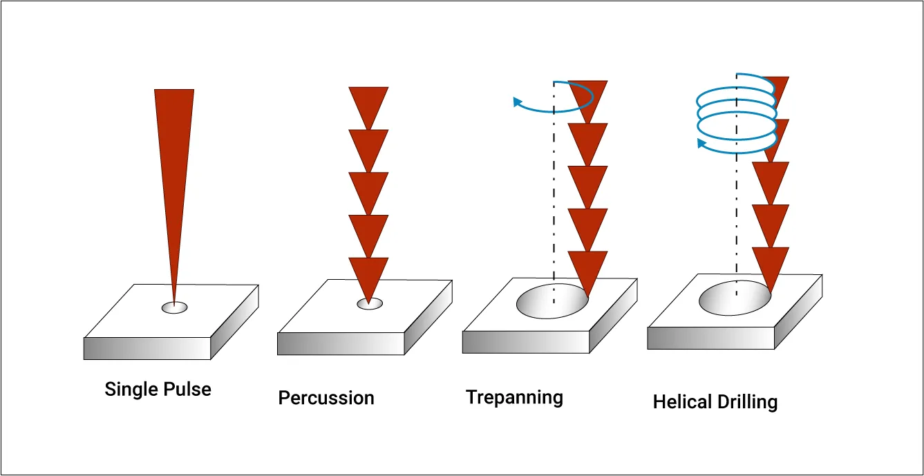
Flexible PCB laser drilling plays a pivotal role, using UV or CO2 lasers to ablate polyimide cleanly without heat-affected zones that could degrade flex life. Laser parameters are tuned for aspect ratios near 1:1, ensuring via walls remain tapered for reliable plating. Post-drilling, desmear processes remove residue, preparing surfaces for metallization. Engineers must consider via capture pad sizes, typically 100-150 microns larger than the drill diameter, to accommodate tolerances.
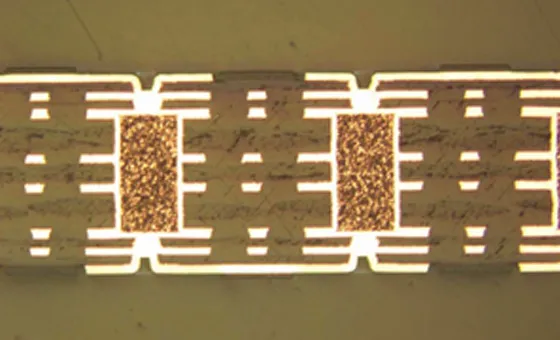
Fine pitch traces require advanced photoresist imaging and etching to achieve uniform linewidths. Etch factors influence undercut, so controlled chemistry prevents line widening at bends. Overall, these principles enable HDI flexible PCBs to handle data rates beyond 10 Gbps while enduring millions of flex cycles.
Manufacturing Processes for HDI Flexible PCBs
Producing HDI flexible PCBs involves specialized sequential build-up processes tailored to handle thin dielectrics and precise features. Initial single-sided or double-sided flex cores are laminated with photosensitive dielectrics, followed by flexible PCB laser drilling for the first microvia layer. Laser ablation creates vias with diameters as small as 75 microns, critical for density. Subsequent copper plating fills vias, and outer layers are patterned using LDI exposure for fine pitch accuracy.
Build-up continues iteratively, with each microvia layer registered to prior ones using fiducials. Stacked vias interconnect multiple levels, while filled vias provide planar surfaces for components. Plasma cleaning enhances adhesion between layers, mitigating delamination risks during flexing. Quality checks per IPC-2223 ensure via integrity through cross-section analysis and electrical testing.
Flexible PCB fine pitch routing demands subtractive or additive patterning, with dry film resists stripped cleanly to avoid residue. Coverlay application protects traces, with windows aligned for surface mounts. Final outlining uses laser routing to preserve edge quality in dynamic areas. These steps yield boards compliant with performance specs, ready for harsh environments.
Challenges arise from material warpage during lamination, addressed by symmetric stackups and low-stress adhesives. Thermal expansion mismatches between copper and polyimide require controlled curing profiles. Yield optimization focuses on laser drill reliability, with inline metrology verifying via dimensions.
Design Best Practices and Practical Solutions
Engineers designing HDI flexible PCBs should prioritize via fanout strategies to escape fine pitch BGAs efficiently. Place microvias under pads where possible, using dog-bone or teardrop shapes for plating relief. Maintain at least 0.1 mm spacing between vias and traces to prevent bridging. IPC-2226 guidelines recommend aspect ratios under 1:1 for blind vias, ensuring plating uniformity.
Bend radius selection is crucial; dynamic areas need radii at least 10 times substrate thickness to avoid fatigue. Position flexible PCB microvias away from flex lines by 1 mm minimum, routing signals perpendicular to bends. Simulate strain using FEA tools to predict crack propagation at via sites. Material selection favors low CTE polyimides for stability across -55°C to 125°C.
For signal integrity, control trace impedance to 50 or 100 ohms with width calculators adjusted for flex dielectric constants around 3.2-3.5. Ground planes shield against EMI, segmented in flex zones to reduce stress. Test prototypes with cyclic bending per industry protocols, iterating on stackup if failures occur.
Power distribution employs filled microvias for low resistance, paralleled where current exceeds 1A per trace. Thermal vias aid heat dissipation in stacked designs. Documentation includes Gerber files with netlists and bend annotations for fabricators.
Troubleshooting Common Issues in HDI Flexible PCBs
Via opens often trace to laser drill misalignment or inadequate desmear, resolved by fiducial optimization and plasma etch verification. Fine pitch shorts result from etch undercut; finer resists and spray etching mitigate this. Delamination in stacks signals poor adhesion, countered by surface activation and cure monitoring.
Flex cracks at microvias indicate high strain; redesign with staggered vias or elastomeric fillers. Signal loss at high frequencies points to dielectric absorption; select lower Dk materials. Production yields improve with DFM reviews early in design.
Conclusion
HDI flexible PCBs excel in maximizing space and performance through innovative microvia integration and fine pitch capabilities. Flexible PCB laser drilling enables precise interconnections, while adherence to standards ensures reliability. Electric engineers benefit from shorter paths for better signals and compact forms for challenging enclosures. Implementing best practices in design and manufacturing unlocks their full potential in next-generation electronics.
FAQs
Q1: What are the key advantages of using HDI flexible PCBs in compact devices?
A1: HDI flexible PCBs provide higher routing density via flexible PCB microvias and fine pitch traces, reducing overall size while preserving flexibility. Shorter interconnects enhance signal integrity and speed, ideal for wearables and sensors. Factory processes align with IPC-6013D for durability under bending and thermal stress. This makes them superior for space-constrained applications requiring high performance.
Q2: How does flexible PCB laser drilling contribute to HDI designs?
A2: Flexible PCB laser drilling creates microvias under 100 microns, enabling stacked interconnects without through-holes. UV lasers ablate polyimide precisely, supporting aspect ratios near 1:1 for plating. This process allows flexible PCB fine pitch routing by freeing surface area. Resulting boards achieve greater layer counts in thin profiles, vital for miniaturization.
Q3: What design considerations apply to flexible PCB fine pitch in HDI?
A3: Flexible PCB fine pitch below 50 microns demands LDI patterning and controlled etching to maintain linewidths. Space vias and traces at least 0.1 mm apart, avoiding bend zones. Use IPC-2226 for via-in-pad rules to support dense BGAs. Simulations predict impedance and strain, ensuring signal quality across flex cycles.
Q4: Can HDI flexible PCBs handle high-frequency signals reliably?
A4: Yes, HDI flexible PCBs minimize via stubs and path lengths for low loss up to multi-GHz. Polyimide dielectrics offer stable Dk, with ground shielding reducing crosstalk. Position flexible PCB microvias strategically to endure flexing without degradation. Standards like IPC-2223 guide testing for consistent performance.
References
IPC-6013D - Qualification and Performance Specification for Flexible Printed Boards. IPC, 2017
IPC-2226 - Design Standard for High Density Interconnect (HDI) Printed Boards. IPC, 2000
IPC-2223 - Sectional Design Standard for Flexible Printed Boards. IPC, 1998


