Introduction
In high-frequency PCB design, achieving optimal performance demands precise control over signal paths and component integration. Buried resistors, embedded directly within the PCB layers, offer a compelling solution by reducing surface clutter and parasitic effects. These high frequency buried resistors integrate seamlessly into multilayer boards, enabling compact layouts essential for RF applications. Engineers face challenges like signal degradation and electromagnetic interference, where traditional surface-mount components introduce unwanted inductance. By leveraging buried resistors, designers can enhance signal integrity in RF circuits while maintaining reliability. This article explores their principles, placement strategies, and best practices for superior high-frequency performance.
What Are Buried Resistors and Why Do They Matter in High-Frequency Design?
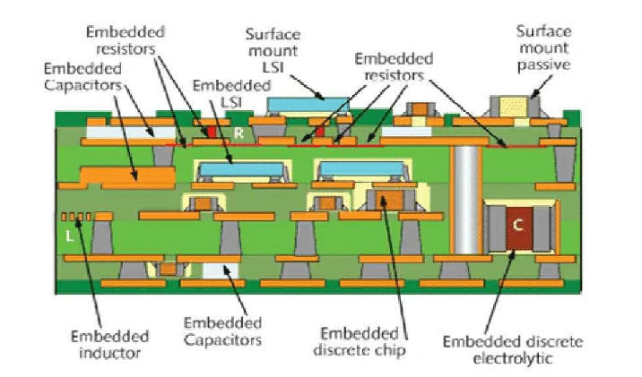
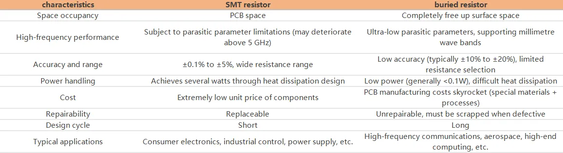
Buried resistors consist of resistive materials, such as thin-film or thick-film formulations, laser-trimmed and embedded between PCB dielectric layers during fabrication. Unlike discrete surface-mount resistors, they eliminate external leads and solder joints, which are primary sources of parasitic inductance. In high-frequency environments above 1 GHz, these parasitics can distort waveforms, leading to reflections and power loss. High frequency buried resistors address this by providing termination or feedback directly at the signal node with minimal interconnect length. Their integration supports denser layouts, crucial for modern RF modules and high-speed digital interfaces. Industry adoption grows as demands for miniaturization and performance intensify in telecommunications and radar systems.
The relevance stems from their ability to preserve signal fidelity where conventional components falter. Parasitic inductance from vias and traces in surface designs amplifies at gigahertz frequencies, degrading return loss and insertion loss metrics. Buried resistors minimize these effects, aligning with the need for controlled impedance environments. They also reduce assembly steps, lowering costs in volume production. For electrical engineers, understanding their fabrication ensures designs meet performance targets without compromising manufacturability.
Technical Principles of Buried Resistors in High-Frequency Applications
Buried resistors operate on the principle of resistive ink or metal alloy deposited on internal copper layers, then encapsulated by dielectrics. Resistance values, typically ranging from tens to thousands of ohms, achieve precision through post-process laser trimming. In high-frequency contexts, their low inductance profile stems from the absence of wire bonds or leads, confining the current path to planar geometry. This geometry reduces self-inductance to picohenry levels, far below discrete equivalents. The surrounding dielectric further shields electromagnetic fields, mitigating crosstalk between adjacent signals.
Signal propagation in RF circuits benefits from this integration, as buried resistors enable precise impedance matching without disrupting trace continuity. Electromagnetic simulations reveal that embedded terminations maintain characteristic impedance better than via-stubbed surface parts. Thermal management improves too, with heat dissipation into inner layers preventing hotspots. Fabrication aligns with IPC-4811 guidelines for embedded passive resistor materials, ensuring material stability under voltage and temperature variations. These principles underpin their superiority in maintaining phase linearity and amplitude flatness across wide bandwidths.
Minimizing Parasitic Inductance with High Frequency Buried Resistors
Parasitic inductance arises primarily from loop areas in component leads and interconnects, manifesting as voltage drops and resonances in high-frequency signals. High frequency buried resistors counteract this by embedding the resistive element coplanar with the signal trace, eliminating vertical transitions. This placement confines magnetic flux within the plane, slashing inductance by orders of magnitude compared to surface-mount devices. Engineers quantify this through inductance formulas, where shorter effective lengths yield sub-pH values ideal for GHz operation.
To minimize parasitic inductance further, designers pair buried resistors with ground planes adjacent to signal layers, forming a stripline configuration. This setup provides a low-impedance return path, suppressing common-mode currents. Vias, if required for access, should employ blind or buried types to avoid through-hole stubs that act as quarter-wave resonators. Controlled dielectric thickness ensures consistent fields, preventing variations that exacerbate inductance. Practical measurements confirm these techniques preserve signal edges, critical for data rates exceeding 10 Gbps or RF bandwidths over 5 GHz.
In RF front-ends, minimizing parasitic inductance directly correlates with improved noise figures and gain flatness. Buried resistors facilitate series or shunt terminations without adding loop inductance, preserving amplifier stability. Compared to discrete parts, they reduce package-related parasitics by 70-90% in typical layouts. Adhering to design rules from IPC-2316 for embedded passives optimizes these benefits during layout.
Enhancing Signal Integrity in RF Circuits Through Buried Resistor Placement
Signal integrity in RF circuits hinges on maintaining waveform shape, minimizing reflections, and controlling crosstalk at elevated frequencies. Buried resistor placement plays a pivotal role, as strategic positioning ensures terminations occur at impedance discontinuity points without excess trace length. For instance, placing them at trace ends for 50-ohm matching prevents standing waves that degrade return loss. Proximity to active devices like transistors reduces stub effects, preserving phase coherence across the band.
Optimal buried resistor placement involves inner layers near high-speed signals, avoiding outer layers prone to radiation. Symmetry in placement relative to differential pairs balances common-mode rejection, vital for mixers and modulators. Layer stackup influences performance, with resistors in signal-ground adjacent pairs offering the best shielding. Engineers must account for tolerance drifts from thermal cycling, specifying materials per established resistor standards. Simulations guide placement to verify eye diagrams and jitter, confirming integrity margins.
Challenges include via minimization, as each adds capacitance and inductance; back-drilling or blind vias mitigate this. Field probing validates post-fabrication integrity, correlating with pre-layout models. Proper placement thus elevates signal integrity in RF circuits, enabling reliable operation in dense, high-power environments.
Best Practices for Implementing Buried Resistors in High-Frequency PCBs
Start with stackup planning, allocating dedicated resistor layers between signal and plane pairs for isolation. Select resistive materials with low temperature coefficients to maintain values under RF power dissipation. Laser trimming post-lamination achieves 1-5% tolerances, essential for precision matching networks. During routing, keep resistor footprints compact, with width-to-length ratios optimizing resistance without excessive area.
Buried resistor placement demands symmetry and minimal vias; integrate them inline with traces where possible. Reference planes must remain continuous beneath, avoiding splits that induce inductance. Thermal vias or heat-spreading copper enhance reliability in power applications. Fabrication partners require design files specifying resistor geometries per IPC-6012E qualification specs for rigid boards. Prototype testing with time-domain reflectometry verifies low reflections.
Document tolerances and trimming windows in fabrication notes to ensure repeatability. Pair with high-frequency laminates featuring low loss tangents for synergistic performance. These practices yield robust designs, minimizing iterations and field failures.
Common Challenges and Troubleshooting Tips
Manufacturing tolerances pose challenges, as resistor values can shift 10-20% pre-trimming due to lamination pressures. Post-trim stability improves with controlled annealing, but humidity sensitivity requires baked panels. In high-power RF, electromigration risks demand wider resistors or higher sheet resistivities. Troubleshooting involves isolating discrepancies via layer peels or X-ray, correlating with process logs.
Signal integrity issues trace to asymmetric placement, causing imbalance; redesign with mirrored layouts resolves this. Overheating manifests as value drift, addressed by derating power below 0.1 W per square. Adhering to standards mitigates most issues, ensuring first-pass success.
Conclusion
Buried resistors revolutionize high-frequency design by minimizing parasitic inductance and bolstering signal integrity in RF circuits. Strategic buried resistor placement near critical nodes unlocks compact, high-performance layouts. Engineers benefit from reduced parasitics, enhanced reliability, and streamlined assembly. Implementing best practices, grounded in industry standards, positions designs for cutting-edge applications. As frequencies climb, these embedded solutions remain indispensable for optimal performance.
FAQs
Q1: What advantages do high frequency buried resistors offer over surface-mount types in RF designs?
A1: High frequency buried resistors reduce parasitic inductance by integrating directly into PCB layers, eliminating leads and solder joints that cause signal distortion. This preserves impedance matching and minimizes reflections in GHz-range circuits. Placement flexibility allows terminations at trace ends without vias, enhancing signal integrity in RF circuits. Overall, they support denser boards with better thermal distribution.
Q2: How does buried resistor placement impact minimizing parasitic inductance?
A2: Buried resistor placement close to signal traces shortens interconnects, confining inductance to planar paths under picohenries. Adjacent ground planes further suppress loop areas, critical for high-speed edges. Avoid outer layers to prevent radiation; inner positions shield effectively. This strategy aligns with design guides for embedded passives, ensuring low-distortion propagation.
Q3: Why are buried resistors essential for signal integrity in RF circuits?
A3: Buried resistors provide precise, low-parasitic terminations that maintain characteristic impedance across bands. Their embedded nature avoids via stubs, reducing return loss and crosstalk. In differential signaling, symmetric placement balances paths for superior common-mode rejection. They excel where surface components introduce excessive inductance, safeguarding waveform fidelity.
Q4: What factors influence effective buried resistor placement in high-frequency PCBs?
A4: Layer proximity to signals, symmetry, and plane continuity dictate effectiveness. Compact geometries minimize area while achieving target values. Material selection per resistor standards ensures stability. Vias should be blind to avoid parasitics. Testing validates placement for real-world integrity.
References
IPC-4811 — Specification for Embedded Passive Device Resistor Materials. IPC
IPC-2316 — Design Guide for Embedded Passive Device Printed Boards. IPC
IPC-6012E — Qualification and Performance Specification for Rigid Printed Boards. IPC, 2017