Introduction
Fitness trackers rely on Bluetooth connectivity to transmit health data reliably in real-time. Designing a Bluetooth antenna directly on the wearable PCB presents unique challenges due to the compact form factor and proximity to the human body. Engineers must balance size constraints with performance to ensure consistent signal strength and low power consumption. This article explores Bluetooth antenna design for wearable PCBs, focusing on key principles for electric engineers. Proper implementation enhances range, reduces interference, and meets regulatory requirements for specific absorption rate limits. By following structured guidelines, designers can achieve reliable operation in dynamic environments like wrist-worn devices.
Why Reliable Bluetooth Antenna Design Matters in Wearable PCBs
Bluetooth operates in the 2.4 GHz ISM band, where wearable devices face interference from Wi-Fi and body tissue absorption. A poorly designed antenna leads to detuned resonance, reduced link budget, and battery drain from retransmissions. In fitness trackers, reliable connectivity supports continuous data syncing during activities, preventing dropouts that frustrate users. Engineers prioritize antenna efficiency to maintain Bluetooth Low Energy protocol advantages, such as extended battery life. Industry demands for smaller devices amplify the need for integrated PCB antennas over discrete chips, as they offer better customization for enclosure shapes. Adhering to established PCB design standards ensures manufacturability and repeatability across production runs.
Bluetooth Antenna Types Comparison for Fitness Trackers
Several antenna types suit the space-constrained, low-profile requirements of fitness trackers. The table below compares popular options for 2.4 GHz Bluetooth applications (approximate values on typical 1.6 mm FR-4 substrate):
| Antenna Type | Typical Dimensions | Efficiency | Pros | Cons | Best For |
|---|---|---|---|---|---|
| Inverted-F Antenna (IFA) | ~7–11 mm × 11–20 mm | High (moderate to high) | Good bandwidth, compact, tunable | Sensitive to ground plane size | General fitness trackers, wearables |
| Meandered Inverted-F (MIFA) | ~5–15 mm × 10–20 mm | Medium to high | Smaller footprint than straight IFA | Slightly narrower bandwidth | Ultra-compact devices |
| Simple Meander Line | ~4 × 20 mm | Medium | Easy to implement, low cost | Lower efficiency, ground sensitive | Cost-sensitive or simple modules |
| Chip Antenna | Very small (e.g., 2–5 mm) | Low to medium | Minimal PCB space, easy integration | Lower efficiency, higher cost | Extremely tight layouts |
Inverted-F variants dominate due to their balance of performance and size, while meander designs help fit slim profiles under watch straps. Selection depends on available board real estate, target range, and enclosure materials.
Fundamentals of Bluetooth Antenna Design for Wearable PCBs
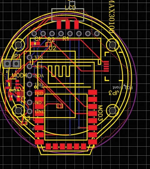
Common PCB antenna types for Bluetooth include inverted-F antennas and meander line structures, suited for limited space in fitness trackers. These trace-based designs leverage the PCB substrate as the radiator, requiring precise trace widths and lengths tuned to quarter-wavelength at 2.4 GHz. Substrate material properties, like dielectric constant, influence velocity factor and resonance frequency, demanding simulation tools for initial sizing. Ground plane size and shape act as a counterpoise, critical for radiation pattern omnidirectionality in wearables. Multi-layer stacks allow routing the feed line under the antenna while maintaining isolation from digital signals. Flexible substrates may be used for curved enclosures, but rigid-flex transitions require careful via placement to avoid losses. Designers should also review flex PCBs for smart eyewear for complementary antenna routing techniques in curved wearables
Bluetooth antenna design for wearable PCBs emphasizes low-profile geometries to fit slim profiles under watch straps. Radiation efficiency drops near the body, so patterns favor perpendicular polarization to the wrist. Keep-out zones prevent components from altering field distribution. Simulations account for enclosure materials, as plastic housings minimally affect signals compared to metal. Prototyping involves vector network analyzer measurements for verification. These principles form the foundation for robust performance in motion-intensive applications.
Optimal Antenna Placement in Fitness Tracker PCBs
Antenna placement in fitness tracker PCBs prioritizes edges or corners to maximize clearance from the ground plane edge. Positioning near the periphery allows unobstructed radiation into free space, improving gain over central locations shrouded by components. Avoid proximity to batteries, displays, or processors, as metal masses detune the antenna and distort patterns. A minimum keep-out area, typically spanning the antenna length plus margins, ensures no vias or traces encroach. In strap-mounted trackers, orient the antenna parallel to the wrist for optimal body decoupling. Multi-antenna setups for diversity require orthogonal placements to mitigate fading.
Layer stackup influences placement, with top-layer traces preferred for minimal via parasitics. Ground vias around the antenna periphery enhance pattern control without excessive coupling. Fitness tracker enclosures often dictate final positioning, so iterative modeling incorporates CAD models. Compliance with IPC-2221 guidelines for trace routing supports signal integrity from transceiver to radiator. Testing in fixture mimicking wrist loading validates choices. Proper antenna placement in fitness trackers thus safeguards link reliability during use. For wearable form factor challenges, see our Ultimate Guide to Flexible PCBs in Wearable Fitness Trackers which covers bend zones and dynamic flex integration with antennas.
Ground Plane, Keep-Out Zones, and Body Loading Effects
The ground plane acts as the antenna’s counterpoise and significantly influences impedance and radiation pattern. A sufficiently large and continuous ground plane improves efficiency, while slots or cuts can be used intentionally for pattern shaping or size reduction.
Strict keep-out zones around the antenna prevent near-field disturbances that alter resonance or efficiency. Visual guidelines often show fenced ground vias spaced at ~λ/20 intervals for better pattern control.
Body loading effects are particularly challenging in wearables: proximity to human tissue (high dielectric constant and lossy) can detune resonance (shifting frequency lower), reduce efficiency by 30–50% or more on-wrist versus free space, and distort radiation patterns due to absorption. Designs often incorporate detuning margins or larger ground planes to compensate. Simulations must include body phantoms (e.g., wrist models) to predict real-world performance accurately.
Achieving Proper PCB Antenna Impedance Matching
PCB antenna impedance matching targets 50 ohms to minimize return loss and maximize power transfer in Bluetooth systems. Feed point impedance varies with geometry, often complex due to capacitive coupling in compact designs. Pi-networks using series inductor and shunt capacitors provide flexibility for tuning across manufacturing tolerances. Smith chart analysis guides component values, aiming for VSWR below 2:1 at 2.4 to 2.48 GHz. Wearable proximity introduces loading, shifting resonance and necessitating detuning margins in initial designs. Production tuning kits allow field adjustments post-assembly.
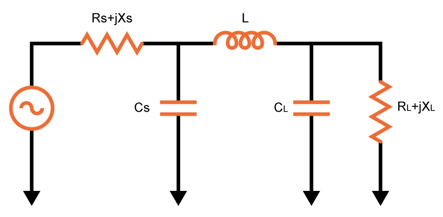
Layout minimizes parasitics by short, wide feed traces controlled to 50 ohms characteristic impedance. Ground return paths use multiple vias for low inductance. Simulations incorporate PCB stackup and component models for accuracy. Measurements confirm S11 below -10 dB, with bandwidth covering the Bluetooth channel. IPC-6012E specifications ensure board quality supports RF performance. Effective PCB antenna impedance matching thus preserves efficiency in wearable environments.
Suggested Reading: Mastering Impedance Matching in PCB Design for Optimal Signal Integrity
Best Practices for RF Layout and Integration
Segregate RF and digital sections with ground stitching to suppress noise coupling into the antenna. Use microstrip or coplanar waveguide for feed lines, calculating widths per stackup for controlled impedance. Vias under the antenna should be fenced with ground returns spaced at lambda/20 intervals. Component placement avoids the near-field region, preserving Q-factor. For fitness trackers, thermal vias dissipate heat without compromising radiator space. Firmware calibration compensates minor variations.
Multi-layer designs route DC power planes away from RF paths, with decoupling capacitors near transceiver pins. Enclosure integration testing evaluates total system efficiency. Adherence to J-STD-020E for moisture sensitivity prevents delamination affecting traces. Documentation includes Gerber files with antenna layers clearly marked. These practices yield production-ready Bluetooth antenna designs for wearable PCBs.
Suggested Reading: PCB RF Antenna Design and Layout Tips
Common Challenges and Troubleshooting in Wearable Designs
Body loading detunes antennas, reducing efficiency by up to 50 percent on-wrist versus free-space. Counter this with larger ground planes or slot modifications for pattern shaping. Manufacturing tolerances shift resonance, addressed by statistical simulations and tuning ranges. Interference from harmonics requires filtering at the transceiver. Overmolding affects dielectric loading, mandating fixture tests. Troubleshooting involves anechoic chamber measurements for pattern and efficiency.
Debugging poor range starts with VNA sweeps for matching, followed by spectrum analysis for spurs. Firmware logs packet error rates to isolate issues. Iterative prototyping refines designs. These steps ensure reliable Bluetooth performance in fitness trackers.
DFM, Manufacturing Tolerances, and Testing Best Practices
Design for manufacturability (DFM) ensures antenna performance survives production variations. Specify tight tolerances on critical trace dimensions and keep-out zones, and include test coupons or tuning pads on panels. Collaborate with fabricators on controlled impedance tolerances and solder mask registration.
Testing best practices include VNA validation on multiple boards, on-body phantom testing, and SAR compliance checks. Environmental testing (temperature, humidity, flex for rigid-flex) verifies stability. Documentation should clearly mark antenna layers in Gerber files. These steps, aligned with standards like IPC-2221 and IPC-6012E, support high-yield, repeatable production of Bluetooth antenna designs for wearable PCBs.
Conclusion
Designing a reliable Bluetooth antenna on a fitness tracker PCB demands attention to placement, matching, and layout principles. Edge positioning, precise impedance control, and isolation practices mitigate wearable challenges. Standards like IPC-2221 and IPC-6012E guide fabrication for consistency. Engineers achieve optimal performance through simulation, prototyping, and testing. This approach delivers seamless connectivity, enhancing user experience in health monitoring devices. Prioritizing these elements positions designs for success in competitive markets.
FAQs
Q1: What are the key considerations for Bluetooth antenna design on wearable PCBs?
A1: Bluetooth antenna design for wearable PCBs focuses on compact inverted-F or meander traces tuned to 2.4 GHz. Substrate choice affects dielectric loading, while body proximity demands efficiency margins. Simulations predict resonance shifts, and edge placement maximizes radiation. Keep-out zones prevent detuning from components. This ensures low power draw and reliable data transfer in fitness applications.
Q2: How does antenna placement impact fitness tracker performance?
A2: Antenna placement in fitness trackers significantly affects range and efficiency by influencing ground plane interaction. Edge or corner locations provide clearance for omnidirectional patterns, avoiding battery shielding. Orientations parallel to the body minimize absorption losses. Keep-outs enforce isolation from noisy circuits. Proper implementation per layout guidelines boosts link budget in dynamic use.
Q3: Why is PCB antenna impedance matching critical for Bluetooth wearables?
A3: PCB antenna impedance matching ensures maximum power transfer, targeting 50 ohms to minimize reflections in Bluetooth wearables. Pi-networks tune complex impedances from trace geometries. Wearable loading requires bandwidth for channel coverage. Poor matching increases VSWR, cutting efficiency and range. Verification via S11 measurements confirms design robustness.
Q4: What standards apply to reliable PCB antenna fabrication?
A4: Standards like IPC-2221 guide trace design and routing for RF integrity. IPC-6012E specifies qualification for rigid boards used in wearables. J-STD-020E addresses moisture handling to prevent warpage affecting antennas. These ensure manufacturability without performance degradation. Compliance supports scalable production for fitness trackers.
References
IPC-2221B — Generic Standard on Printed Board Design. IPC, 2012
IPC-6012E — Qualification and Performance Specification for Rigid Printed Boards. IPC, 2017
J-STD-020E — Moisture/Reflow Sensitivity Classification for Nonhermetic Surface Mount Devices. JEDEC, 2014


