Introduction
Organic PCBs play a pivotal role in modern electronics where high-frequency signals demand precise control over signal integrity. As data rates climb into the gigahertz range, engineers face challenges in maintaining low signal loss and minimal distortion using cost-effective organic substrates. These materials, primarily polymer-based laminates reinforced with glass fibers, offer a balance between performance and manufacturability compared to inorganic alternatives. This article explores design considerations and material selection strategies for achieving superior high-frequency performance with organic PCBs. Key factors such as dielectric properties and stackup geometry directly influence outcomes in applications like 5G infrastructure and high-speed computing. By adhering to established guidelines, designers can optimize organic PCB high frequency capabilities without compromising reliability.
Understanding Organic PCBs in High-Frequency Contexts
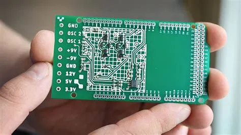
Organic PCBs refer to printed circuit boards constructed with organic dielectric materials, typically epoxy resins or polyimides combined with fiberglass reinforcement. These substrates dominate high-speed PCB organic designs due to their versatility, scalability, and lower cost relative to ceramics. In high-frequency environments above 1 GHz, the material's electrical characteristics become critical for preserving signal quality over long traces. Unlike standard FR-4 suited for lower speeds, advanced organic laminates provide enhanced properties tailored for demanding signals. The shift toward organic PCB high frequency solutions stems from the need for multilayer boards that support dense routing while managing heat and mechanical stress. Engineers must evaluate these boards through the lens of signal propagation and loss mechanisms to ensure robust performance.
Key Technical Principles Governing Performance
Signal integrity in organic PCBs hinges on the dielectric constant, which dictates the speed of electromagnetic wave propagation. A lower dielectric constant reduces propagation delay, allowing signals to travel closer to the speed of light in vacuum. For high-speed PCB organic applications, materials with dielectric constants below typical values help minimize skew between differential pairs. Dissipation factor, or loss tangent, quantifies energy converted to heat, directly impacting attenuation at higher frequencies. Organic substrates with low dissipation factors preserve amplitude and phase fidelity, crucial for eye diagram quality. Variations in these properties across temperature and humidity further complicate designs, necessitating stable formulations.
Crosstalk arises from capacitive and inductive coupling between adjacent traces, exacerbated in high-density organic layouts. Proper trace spacing and grounding mitigate mutual inductance effects. Reflections occur due to impedance discontinuities at vias, bends, or terminations, leading to ringing and overshoot. Controlled impedance design, guided by IPC-2221 standards for organic printed boards, ensures characteristic impedance matches driver and receiver requirements. Skin effect confines current to trace surfaces at high frequencies, increasing effective resistance and loss. Vias introduce parasitic inductance and capacitance, demanding optimized stub lengths and back-drilling techniques.
Material Selection Criteria for Low-Loss Organic Substrates
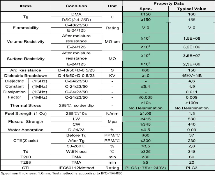
Selecting a low loss PCB substrate begins with prioritizing dielectric constant and dissipation factor suited to the operating frequency. Organic materials engineered for high frequency exhibit stable dielectric constants with minimal variation over broad bandwidths. Low dissipation factors, typically targeted for minimal values, reduce insertion loss in transmission lines. Thermal coefficient of dielectric constant influences performance under operational heat, preventing shifts in timing budgets. Coefficient of thermal expansion matching between layers avoids warpage and delamination in multilayer stacks.
Mechanical stability is equally vital, as organic substrates must withstand fabrication stresses like lamination and drilling. Glass transition temperature indicates rigidity post-cure, affecting via reliability. Moisture absorption alters electrical properties, so low absorption rates are preferred for humid environments. Per IPC-2222 guidelines for rigid organic boards, material qualification involves verifying these parameters through standardized tests. Cost and availability guide final choices, balancing exotic low-loss organics against volume production needs. Engineers often compare datasheets focusing on frequency-specific Dk and Df curves.
Design Considerations for Optimal High-Frequency Performance
Stackup design forms the foundation of signal integrity organic PCB layouts. Symmetric builds with balanced copper weights minimize bow and twist, ensuring consistent dielectric thickness. Core and prepreg selection must align Dk values to prevent intra-pair skew in differential signaling. Ground planes adjacent to signal layers provide return paths, reducing loop inductance and EMI. For high-speed PCB organic routing, microstrip or stripline configurations offer controlled impedance with formulas accounting for substrate height and width.
Trace geometry optimization involves wider lines for lower loss and serpentine patterns for length matching. Via design favors blind or buried types to shorten stubs, with IPC-6012 qualification ensuring plating integrity. Power distribution networks require decoupling capacitors near ICs to stabilize voltage rails. Thermal vias and copper pours manage heat from high-frequency operation. Simulation tools verify pre-layout performance, predicting insertion loss and crosstalk. Fabricators input on drill aspect ratios and panelization refines manufacturability.
Routing high-speed signals away from edges reduces fringing fields, while stitching vias tie ground planes. Reference plane splits demand smooth transitions to avoid impedance bumps. For organic PCB high frequency boards, enclosure shielding complements internal design. Post-layout reviews confirm adherence to design rules derived from material properties.
Best Practices and Troubleshooting Insights
Implement length tuning and phase alignment during routing to equalize propagation delays. Use serpentine meanders judiciously, avoiding sharp bends that introduce radiation. Pre-emphasis and equalization at drivers compensate for channel loss in longer traces. Factory trials validate material performance under real process conditions. Troubleshooting distorted signals often traces to via resonances; resonance mitigation via back-drilling resolves this.
Adopt a co-design approach integrating PDN and SI early. Reference IPC-2221 for baseline rules on clearance and creepage in high-density areas. Monitor fabrication tolerances for dielectric thickness, as variations amplify losses. Field returns highlight humidity effects, prompting conformal coatings. Iterative prototyping refines designs, correlating simulations with measurements.
Conclusion
Achieving high-frequency performance with organic PCBs demands meticulous attention to material selection and design details. Low dielectric constant organic PCB materials and low loss substrates enable reliable signal integrity at gigahertz speeds. Structured approaches to stackup, routing, and verification yield robust high speed PCB organic solutions. By leveraging standards like IPC-2221 and IPC-2222, engineers mitigate common pitfalls effectively. Future advancements in organic formulations promise even better trade-offs, sustaining this technology's relevance. Prioritizing these considerations ensures designs meet stringent performance targets.
FAQs
Q1: What role does dielectric constant play in organic PCB high frequency performance?
A1: Dielectric constant determines signal propagation speed in organic substrates, with lower values reducing delay and skew. For high-frequency applications, stable Dk across frequencies preserves timing margins. Engineers select materials with appropriate Dk to match impedance requirements. This parameter directly impacts signal integrity organic PCB outcomes, especially in multilayer stacks. Proper selection aligns with design goals for minimal distortion.
Q2: How do you ensure signal integrity in high speed PCB organic designs?
A2: Signal integrity relies on controlled impedance traces, solid reference planes, and low-loss dielectrics. Minimize vias and optimize spacing to curb crosstalk and reflections. Simulations predict issues like attenuation before fabrication. Adhering to IPC guidelines ensures manufacturable layouts. These practices maintain clean eye patterns at multi-GHz rates.
Q3: What makes a low loss PCB substrate ideal for high-frequency organic PCBs?
A3: Low loss substrates feature minimal dissipation factor to limit signal attenuation as heat. Combined with low Dk, they support long traces without excessive degradation. Thermal and mechanical stability prevents performance shifts. Selection focuses on frequency-specific data for targeted applications. This enables reliable organic PCB high frequency operation.
Q4: Why is stackup symmetry critical for high-frequency organic PCBs?
A4: Symmetric stackups balance copper and dielectric layers, preventing warpage and thickness variations. Consistent dielectric spacing ensures uniform impedance control. This reduces intra-layer skew in high-speed signals. Factory processes align better with symmetric builds per standards. Overall, it enhances signal integrity organic PCB reliability.
References
IPC-2221B — Generic Standard on Printed Board Design. IPC, 2012
IPC-2222B — Sectional Design Standard for Rigid Organic Printed Boards. IPC, 2015
IPC-6012E — Qualification and Performance Specification for Rigid Printed Boards. IPC, 2017


