Introduction
Ultra-thin printed circuit boards play a critical role in the evolution of flexible electronics, enabling compact designs for applications like wearables, medical devices, and consumer gadgets. These boards typically feature thicknesses below 0.5 mm, often as low as 0.1 mm, which demands specialized manufacturing approaches to maintain reliability and performance. The ultra-thin PCB manufacturing process introduces unique hurdles, including material fragility, precision requirements, and thermal sensitivities that can compromise yield rates. Engineers must address these issues to harness the benefits of flexibility and space savings in modern electronics. This article explores the primary challenges and proven strategies drawn from factory practices, focusing on handling, drilling, warping prevention, and cost optimization.
What Are Ultra-Thin PCBs and Why They Matter in Flexible Electronics
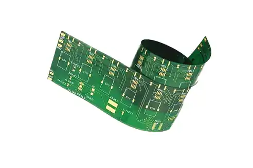
Ultra-thin PCBs consist of substrates with core thicknesses under 0.5 mm, often using polyimide or other flexible dielectrics clad with thin copper foils. They differ from standard rigid boards by prioritizing bendability while supporting high-density interconnects through microvias and fine-line traces. In flexible electronics, these boards allow dynamic form factors that conform to curved surfaces or foldable structures, essential for advancing IoT devices and sensors. Their relevance stems from the push for miniaturization, where traditional boards exceed space constraints in slim profiles. Factory insights reveal that ultra-thin designs reduce overall assembly height by up to 70 percent in stacked configurations, enhancing portability without sacrificing functionality. Compliance with established guidelines ensures these boards withstand repeated flexing cycles in real-world use.
Key Challenges in the Ultra-Thin PCB Manufacturing Process
The ultra-thin PCB manufacturing process amplifies risks at every stage, from material preparation to final lamination. Thin substrates lack inherent rigidity, leading to issues like tearing during transport or misalignment in etching. Thermal expansions during pressing create internal stresses that propagate defects. High-density features require sub-100 micron vias, pushing equipment limits. Yield losses from these factors can exceed 20 percent without optimized controls, underscoring the need for precise process management. Factory-driven approaches emphasize proactive mitigation to sustain production scalability.
Handling Thin PCB Materials
Handling thin PCB materials presents the foremost challenge due to their susceptibility to mechanical damage and contamination. Panels under 0.2 mm warp or crease under minimal pressure, complicating automated transport in cleanrooms. Dust particles adhere easily to exposed surfaces, risking shorts during imaging or plating. Standard carriers fail as thin stacks shift during indexing, causing scratches or delamination. Operators must employ vacuum-assisted fixtures to secure panels without direct contact. Protective films applied post-etching prevent handling-induced defects, a practice aligned with storage guidelines for fragile boards.
Engineers recommend limiting stack heights to 10-12 boards during drilling to avoid compression damage. ESD-compliant trays with rigid backings support odd-shaped flex panels, reducing impact risks. Pre-handling inspections verify flatness using non-contact gauges before processing. These techniques minimize rejects by maintaining material integrity throughout the workflow.
Microvia Drilling Techniques
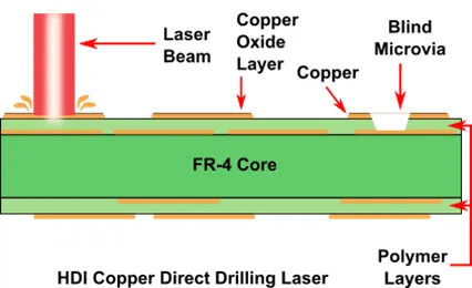
Microvia drilling techniques demand high precision for ultra-thin layers, where mechanical drills falter below 150 microns. Laser ablation, using CO2 or UV wavelengths, vaporizes dielectrics cleanly without burrs, achieving aspect ratios near 1:1. However, heat-affected zones can carbonize polyimide, leading to residue buildup that impedes plating adhesion. Stacked vias in multilayer flex risk misalignment if entry-exit registration exceeds 25 microns. Factories optimize pulse durations to balance speed and hole quality, often combining YAG lasers for copper breakthrough. Post-drill desmearing with plasma ensures via walls accept electroless copper uniformly.
Challenges intensify in blind vias spanning partial layers, requiring sequential drilling to prevent taper. Aspect ratios above 0.8:1 increase breakthrough times, elevating costs. Routine verification via cross-sectioning confirms barrel integrity before fill. These methods enable HDI densities critical for flexible electronics signals.
Minimizing Warping in Thin PCBs
Minimizing warping in thin PCBs requires addressing asymmetric stresses from copper distribution and hygroscopic swelling. Uneven foil patterns induce bow exceeding 0.75 percent during lamination, propagating to assembly failures. Reflow profiles amplify curvature as glass transition temperatures vary across layers. Moisture absorption prior to pressing causes delamination, with thin cores retaining vapor longer. Factories counter this by symmetric stackups, balancing copper weight on both sides. Pre-baking at 120-150 degrees Celsius for 4-6 hours expels volatiles, aligning with handling protocols.
Cooling rates post-lamination influence residual stresses; gradual ramps prevent thermal gradients. Fixtures during solder mask cure clamp panels flat, reducing twist to under 0.5 percent. High-Tg materials above 170 degrees Celsius resist softening in lead-free processes. Storage in humidity-controlled environments below 50 percent RH preserves planarity. These interventions ensure boards meet performance specs under flex cycles.
Best Practices for Overcoming Manufacturing Hurdles
Implementing best practices transforms challenges into reliable processes in ultra-thin PCB production. Start with design-for-manufacturability reviews, specifying bend radii at least 10 times substrate thickness to avoid cracking. Material selection favors low-CTE polyimides matching copper expansion coefficients. Process controls include real-time monitoring of etch rates for fine lines under 50 microns. Plasma cleaning replaces wet desmear for residue-free vias, boosting yields.
For assembly compatibility, incorporate stiffeners at connector sites without compromising flex zones. Inline metrology verifies via fills post-electroplating, catching voids early. These factory-aligned steps enhance throughput while upholding quality.
Strategies for Cost-Effective Thin PCB Production
Cost-effective thin PCB production hinges on optimizing volume, design, and tooling. Panelization maximizes substrate utilization, yielding 4-6 times more boards per sheet for small outlines. Reducing layer counts via blind vias cuts lamination cycles, a key driver of expenses. Standardized stackups minimize custom tooling, spreading setup costs across runs. Laser drilling, though capital-intensive, accelerates microvia formation over mechanical methods, lowering per-hole costs at scale.
Bulk material procurement secures thin foils at volume discounts, while DFM feedback loops iterate designs pre-production. Yield improvements from warping controls recoup investments quickly. Low-volume runs benefit from shared panels, amortizing NRE fees. These tactics deliver prototypes economically without quality trade-offs.
Ensuring Compliance and Quality in Ultra-Thin PCB Manufacturing
Quality control in ultra-thin manufacturing adheres to IPC-6013 for flexible board qualifications, specifying bow and twist limits under 0.5 percent. IPC-2223 guides sectional designs, ensuring via reliability in flex zones. IPC-1601 outlines handling protocols, mandating protective measures for thin panels to prevent ESD and mechanical damage. Cross-verification via thermal cycling tests confirms performance post-process. Factories integrate these standards into SPC charts, tracking CpK above 1.33 for critical features. Such diligence guarantees field reliability in demanding applications.
Conclusion
Manufacturing ultra-thin PCBs for flexible electronics demands mastery over handling thin PCB materials, advanced microvia drilling techniques, and strategies for minimizing warping in thin PCBs. Factory insights emphasize symmetric designs, laser precision, and controlled environments to overcome fragility and stresses. Cost-effective thin PCB production leverages panelization and DFM for scalability. By integrating standards like IPC-6013, engineers achieve high yields and robust performance. These practices position flexible electronics for broader adoption in compact, dynamic systems.
FAQs
Q1: What are the main steps in the ultra-thin PCB manufacturing process?
A1: The ultra-thin PCB manufacturing process begins with thin foil lamination, followed by imaging and etching for fine traces. Laser drilling forms microvias, then plating fills interconnects. Lamination builds multilayers, with final steps including solder mask and testing. Strict controls on temperature and handling ensure planarity throughout. This sequence supports high-density flexible designs reliably.
Q2: How can engineers improve handling thin PCB materials during production?
A2: Handling thin PCB materials improves with rigid carriers and vacuum fixtures to prevent shifting or creasing. Protective backings and ESD trays safeguard against impacts, per IPC-1601 guidelines. Limit stacking to 12 panels max during drilling and use non-contact transport. Pre-inspections detect warpage early. These methods reduce defects significantly in factory settings.
Q3: What microvia drilling techniques work best for minimizing warping in thin PCBs?
A3: Microvia drilling techniques like UV laser ablation minimize warping in thin PCBs by limiting heat zones and ensuring clean entries. Sequential blind via formation avoids deep penetration stresses. Post-drill plasma desmear maintains flatness for plating. Optimized pulses balance speed and quality, preventing carbonization. This approach integrates well with warping controls for stable multilayers.
Q4: What strategies ensure cost-effective thin PCB production?
A4: Cost-effective thin PCB production uses panelization to maximize yield per sheet and DFM to simplify layers. High-Tg materials reduce rework from thermal issues. Bulk foils and standardized processes lower per-unit costs. Laser drilling scales efficiently for microvias. Yield-focused handling cuts waste, making ultra-thin flex viable for mid-volumes.
References
IPC-6013DS — Qualification and Performance Specification for Flexible and Rigid-Flex Printed Boards. IPC, 2014
IPC-2223C — Sectional Design Standard for Flexible/Rigid-Flexible Printed Boards. IPC, 2019
IPC-1601A — Printed Board Handling and Storage Guidelines. IPC, 2021


