Introduction
Hearing Aids Printed Circuit Boards represent a pinnacle of miniaturization in electronics, where every trace and via must perform flawlessly within the tight confines of an ear canal device. These PCBs handle analog audio signals, digital processing, and wireless communications, all while prioritizing biocompatibility and reliability. Impedance control emerges as a critical factor, ensuring signal integrity across high-frequency paths to prevent degradation that could impair hearing clarity. Engineers face a massive selection of design options, from rigid-flex hybrids to HDI structures, each tailored to balance performance with form factor constraints. This article explores the engineering principles behind Hearing Aids Printed Circuit Boards with impedance control, addressing key challenges like signal interference and maintaining effective file transfer rates in wireless features. By understanding these elements, electronic engineers can optimize designs for superior patient outcomes.
What Is a Hearing Aids Printed Circuit Board and Why Impedance Control Matters
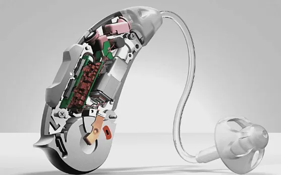
A Hearing Aids Printed Circuit Board integrates components for microphone input, signal amplification, digital signal processing, and output to receivers, often in volumes smaller than a fingertip. These boards typically employ high-density interconnects, fine-line traces under 50 microns, and multilayer stackups to accommodate batteries, antennas, and ASICs. Impedance control refers to designing and fabricating traces with a specified characteristic impedance, usually 50 or 100 ohms differential, to match source and load conditions. Without it, mismatches cause reflections that distort signals, leading to crosstalk or attenuation in audio paths. In hearing aids, where wireless links enable streaming or pairing, poor impedance control amplifies signal interference, reducing effective file transfer rates for data like firmware updates. This control matters because it directly impacts the device's ability to deliver clear sound in noisy environments, aligning with reliability demands for prolonged wear.
The massive selection available stems from varied material dielectrics, copper weights, and layer counts, allowing engineers to select configurations for specific frequency bands. For instance, RF sections for Bluetooth require tighter tolerances than baseband audio lines. Industry standards like IPC-2141 provide guidelines for calculating and verifying controlled impedance in such high-speed designs. Ultimately, impedance control ensures the PCB supports the full spectrum of hearing aid functions without compromising on size or power efficiency.
Technical Principles of Impedance Control in Hearing Aids PCBs
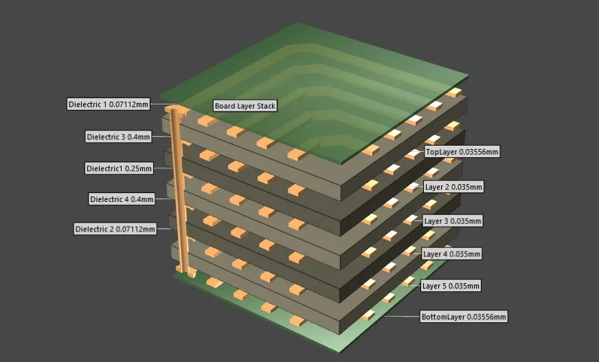
Impedance in a PCB trace arises from its geometry and surrounding dielectric, modeled as transmission lines in microstrip or stripline configurations. Microstrip traces, exposed on outer layers, suit shorter runs but couple more to air, while striplines embedded between ground planes offer better shielding against external noise. Key parameters include trace width, thickness, dielectric height, and material constant (Dk), all interdependent in stackup planning. Engineers use field solvers to predict impedance, iterating designs to hit targets within 10% tolerance. In Hearing Aids Printed Circuit Boards, these principles apply to RF antennas and high-speed digital buses, where even minor deviations elevate signal interference.
For differential pairs common in balanced audio outputs, symmetric routing maintains equal impedances, minimizing common-mode noise. Dielectric materials with low loss tangent (Df) preserve signal energy at gigahertz frequencies used in wireless hearing aids. Fabrication involves precise etching and lamination to replicate simulations, with test coupons providing verification points. Signal reflections from discontinuities like vias or bends degrade waveform integrity, directly affecting file transfer rates in data-intensive operations. Proper impedance control thus forms the backbone of robust signal propagation in these compact assemblies.
Hearing aids often incorporate rigid-flex transitions, where impedance must remain consistent across material boundaries to avoid step changes. Ground plane stitching vias return currents efficiently, reducing loop inductance that exacerbates interference. These technical facets enable engineers to navigate the massive selection of PCB variants confidently.
Challenges in Hearing Hids PCBs: Signal Interference and File Transfer Rates
Signal interference plagues Hearing Aids Printed Circuit Boards due to dense packing of analog, digital, and RF sections, fostering crosstalk between adjacent traces. Electromagnetic coupling induces noise on sensitive audio lines from switching digital circuits, while external sources like cell phones add ingress. Impedance discontinuities amplify these effects, converting minor perturbations into bit errors or audio artifacts. In wireless models, 2.4 GHz bands contend with Wi-Fi, demanding low-noise floors for reliable links. Engineers must partition sections with guard traces or moats to isolate domains effectively.
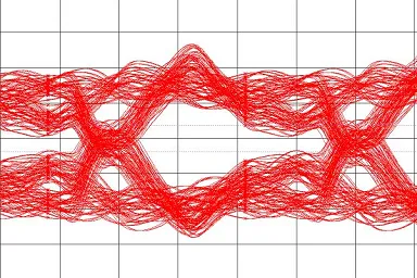
File transfer rates, crucial for streaming audio or bidirectional data exchange, suffer when interference elevates packet error rates, throttling throughput. Mismatched impedances cause overshoot and ringing, violating eye diagram margins in high-speed protocols. Power supply noise couples through planes, further degrading margins in battery-constrained designs. Miniaturization exacerbates parasitics, making every routing decision pivotal. Addressing these requires holistic simulation from schematic to layout, verifying against real-world stressors.
Practical Solutions and Best Practices for Impedance-Controlled Hearing Aids PCBs
Start with stackup definition early, allocating layers for power/ground planes sandwiching signal routes for stripline benefits. Specify impedance requirements per net class in design files, including tolerances like +/- 10%. Collaborate with fabricators on material selection, favoring low-Dk laminates for RF sections. Include TDR test coupons at board edges for post-etch verification, ensuring production matches design. For Hearing Aids Printed Circuit Boards, prioritize via-in-pad for density while back-drilling stubs to preserve impedance.
Routing practices include length-matched pairs, avoiding right-angle bends, and ample spacing per IPC-A-600 guidelines for class 3 assemblies. Ground flooding with dense vias suppresses resonances, curbing signal interference. Simulate mixed-signal interactions to predict and mitigate crosstalk, adjusting trace separation dynamically. In manufacturing, controlled etching processes maintain line width uniformity, critical for impedance stability. The massive selection of options allows tailoring to prototypes or volume runs, with quick-turn capabilities for iterations.
Firmware and protocol layers benefit indirectly, as clean analog fronts enable higher file transfer rates without retransmissions. Regular DFM reviews catch issues like drill breakout affecting ground integrity. Adhering to IPC-6012 performance specs guarantees qualification for extended life cycles. These steps empower engineers to deliver interference-free performance reliably.
Troubleshooting Common Issues in Impedance-Controlled Designs
Electronic engineers often encounter impedance drift from plating variations or dielectric inconsistencies during prototyping. Verify with flying probe tests early, correlating to simulation models for root cause analysis. Signal interference spikes may trace to unstitched ground returns; add vias iteratively until coupling drops. For file transfer rate drops, inspect eye patterns at receiver ends, tweaking equalization if supported. Flex regions demand extra care, as bend radii alter effective dielectric spacing.
Layer misalignment in multilayers shifts reference plane distances, inflating impedance; X-ray inspections confirm registration. Power integrity ties in, with decap placement near ICs stabilizing supplies against ripple-induced interference. Document lessons in design rules for reuse across the massive selection of Hearing Aids Printed Circuit Board variants. Systematic debugging preserves signal margins under real usage.
Conclusion
Hearing Aids Printed Circuit Boards with impedance control demand precision across design, fabrication, and verification to conquer miniaturization hurdles. Key to minimizing signal interference and sustaining file transfer rates lies in disciplined stackup planning, routing, and testing aligned with standards like IPC-2141 and IPC-6012. The massive selection of configurations offers flexibility for evolving wireless and DSP needs, enabling engineers to craft devices that enhance hearing fidelity. Prioritizing these practices ensures reliable, high-performance outcomes in a competitive field. Future advancements in materials will further refine these capabilities, but foundational engineering rigor remains paramount.
FAQs
Q1: What role does impedance control play in reducing signal interference on Hearing Aids Printed Circuit Boards?
A1: Impedance control matches trace characteristics to signal sources, preventing reflections that couple noise between lines. In dense layouts, this minimizes crosstalk, especially near RF antennas. Engineers achieve this through precise stackups and verification, ensuring clean audio paths amid digital switching. Overall, it upholds signal-to-noise ratios vital for clear hearing reproduction.
Q2: How does impedance mismatch affect file transfer rates in wireless hearing aids PCBs?
A2: Mismatch induces waveform distortion, increasing bit errors in data streams like Bluetooth audio. This forces retransmissions, effectively lowering file transfer rates despite nominal protocol speeds. Proper control via test coupons and TDR maintains integrity for seamless pairing and updates. Engineers simulate paths to preempt such degradations early.
Q3: Why is a massive selection important for Hearing Aids Printed Circuit Board designs?
A3: Varied options in layers, materials, and flex integration allow customization to specific frequency needs and form factors. This accommodates evolving features like LE Audio without redesigns. Selection based on impedance specs ensures compatibility across prototypes to production. It streamlines development for electronic engineers targeting reliability.
Q4: What best practices ensure impedance control in manufacturing Hearing Aids Printed Circuit Boards?
A4: Define net classes with tolerances, include coupons, and select low-loss dielectrics. Fabricate under IPC class 3 for medical reliability, verifying post-etch. Route symmetrically for differentials, stitching grounds densely. These steps combat signal interference, supporting high file transfer rates in compact devices.
References
IPC-2141 — Controlled Impedance Circuit Boards and High Speed Logic Design. IPC.
IPC-6012E — Qualification and Performance Specification for Rigid Printed Boards. IPC, 2017.
IPC-A-600K — Acceptability of Printed Boards. IPC, 2020.


