Introduction
Fitness devices have evolved into sleek, lightweight wearables that track heart rates, steps, and sleep patterns with remarkable precision. Engineers face the challenge of packing advanced sensors, processors, and batteries into ever-smaller form factors while maintaining reliability and performance. PCB miniaturization techniques for wearables address these demands by enabling higher component density without sacrificing functionality. This article explores proven strategies for designing compact PCBs in fitness trackers, focusing on high-density interconnect PCB fitness tracker applications and component placement strategies for wearable PCBs. By mastering these techniques, designers can optimize space, reduce weight, and enhance user comfort in devices worn 24/7. The principles discussed here draw from established engineering practices to guide electric engineers toward robust solutions.
Why PCB Miniaturization Matters for Compact Fitness Devices
Compact fitness devices prioritize portability and ergonomics, where every millimeter counts toward battery life and wearability. Larger PCBs lead to bulkier enclosures, compromising the seamless integration into wristbands or chest straps. Miniaturization allows for thinner profiles, distributing heat more effectively during prolonged use and improving signal integrity in noisy environments. For instance, fitness trackers must withstand sweat, motion artifacts, and varying temperatures, making reliable interconnections critical. PCB miniaturization techniques for wearables thus directly impact device longevity and user satisfaction. Engineers must balance density with manufacturability to avoid yield losses in production.
High-density interconnect PCB fitness tracker designs exemplify this balance, supporting microcontrollers alongside accelerometers and optical sensors in minimal footprints. Without strategic miniaturization, devices risk overheating or electromagnetic interference, degrading accuracy in biometric readings. Industry trends show a shift toward sub-1mm pitch components, demanding precise layout rules. These factors underscore the need for systematic design approaches that prioritize both performance and cost-efficiency. Ultimately, effective miniaturization ensures fitness devices meet consumer expectations for unobtrusive, all-day monitoring.
Core Principles of PCB Miniaturization Techniques for Wearables
Miniaturization begins with substrate selection and layer optimization, where thinner cores and prepregs reduce overall board thickness. Microvias, typically under 150 microns in diameter, enable vertical interconnections in stacked configurations, freeing surface area for components. Laser-drilled vias offer superior precision compared to mechanical drilling, minimizing aspect ratios for reliable plating. These techniques align with IPC-6016 standards for high-density interconnect boards, ensuring controlled impedance and minimal crosstalk. Engineers must model signal paths early to predict losses in high-frequency biometric signals.
Component scaling plays a pivotal role, with 0201 and 01005 packages dominating wearable designs for their low profiles. Fine-line traces, often 50 microns wide, require advanced imaging processes to maintain etch uniformity. Build-up processes layer dielectrics sequentially, allowing embedded passives that shrink footprints further. Thermal expansion mismatches demand careful material pairing to prevent delamination under cyclic stresses from body movement. By adhering to these principles, PCB miniaturization techniques for wearables achieve densities exceeding 100 components per square centimeter.
Signal integrity principles guide trace routing, emphasizing length matching for differential pairs in sensor interfaces. Ground planes shield against EMI from arm swings or nearby electronics. Power distribution networks use decoupling capacitors placed within 100 microns of IC pins to stabilize voltage rails. These mechanisms collectively enable high-density interconnect PCB fitness tracker functionality in constrained spaces.
High-Density Interconnect PCBs for Fitness Trackers
High-density interconnect (HDI) PCBs revolutionize fitness tracker designs by supporting blind, buried, and stacked vias for complex routing. Any-layer HDI configurations connect all layers without traditional through-holes, ideal for multi-sensor integration. Sequential build-up fabricates these structures, with filled vias preventing solder wicking during assembly. IPC-6016 qualification verifies via reliability through thermal cycling and shear testing, critical for devices exposed to body heat fluctuations. Designers specify via-in-pad for BGA components, enhancing density while managing parasitics.
Fitness trackers benefit from HDI's ability to embed resistors and capacitors directly into the dielectric, reducing board real estate by up to 30 percent in optimized layouts. Microstrip and stripline geometries control characteristic impedance for I2C and SPI buses common in wearables. Copper foil thickness, typically 1 oz or less, supports narrow traces without excessive resistance. Plating uniformity ensures low via resistance, vital for low-power modes extending battery life.
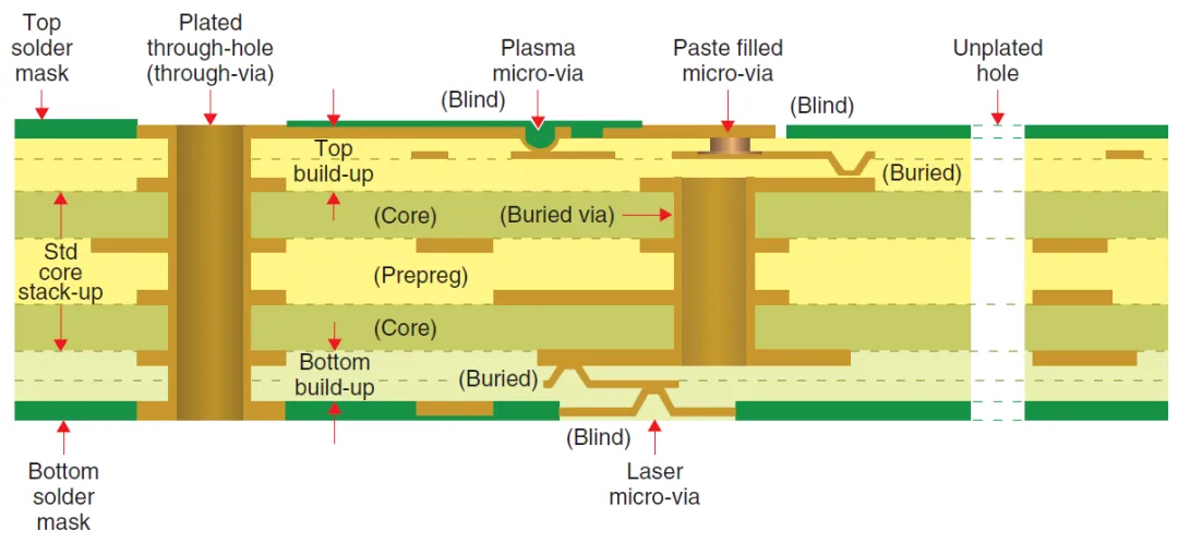
Substrate-like PCBs (SLP) extend HDI principles with ultra-thin cores under 50 microns, mimicking IC packaging. These suit premium fitness devices with integrated displays and haptics. Laser direct imaging patterns finer features, achieving 25-micron lines and spaces. Engineers validate designs through finite element analysis for warpage, as thin stacks warp under reflow stresses.
Component Placement Strategies for Wearable PCBs
Strategic component placement optimizes thermal dissipation and mechanical stability in wearable PCBs. Position heat-generating ICs near board edges for convective cooling against skin or air. Group analog sensors away from digital noise sources, using guard traces to isolate signals. Density rules dictate 0.3mm minimum clearances between pads, preventing bridging in high-volume assembly.
For fitness trackers, centralize the microcontroller to minimize trace lengths, reducing latency in data processing. Battery connectors anchor at corners to counter flexing from wrist motion. Passive components cluster near power pins, forming distributed filters against ripple. These component placement strategies for wearable PCBs enhance signal-to-noise ratios in photoplethysmography sensors.
Prioritize bottom-side mounting for discretes, reserving top surfaces for user-facing interfaces. Symmetry in placement mitigates warpage, aligning with J-STD-020 guidelines for moisture sensitivity. Simulate airflow paths during design to avoid hotspots exceeding 85 degrees Celsius on skin-contact areas. Iterative placement refines routing congestion, ensuring escape routes for fine-pitch BGAs.
Best Practices for Implementing Miniaturization in Design
Adopt a layered stackup with symmetric builds to control CTE mismatches, using low-loss dielectrics for RF sections. Simulate impedance profiles across frequencies up to 100 MHz for Bluetooth modules. Employ teardrop pads on vias to reduce stress concentrations during thermal ramps. Panelization strategies during fabrication maximize yield for small boards under 50x50mm.
Test prototypes with flying probe for opens and shorts, followed by X-ray for BGA voids. Reflow profiling per IPC-A-610 ensures consistent solder joints in HDI assemblies. Document design rules in a database for team consistency, including annular ring specs of 75 microns minimum.
Firmware considerations integrate with hardware, enabling dynamic power gating for idle sensors. Collaborate with fabricators early on DFM checks, verifying drill sizes and panel yields. These practices solidify PCB miniaturization techniques for wearables in production-ready designs.
Common Challenges and Troubleshooting Insights
Warpage emerges in thin HDI stacks due to asymmetric copper distribution, detectable via shadow moire per IPC-TM-650. Counter this with balanced routing and fixture supports during reflow. Solder mask registration errors on fine features cause opens; specify laser-cut stencils with 1:1 aperture-to-pad ratios.
Via failures from plating cracks plague high-aspect microvias; electropolishing post-plating smooths surfaces. Debug signal crosstalk by adding stitching vias along reference planes. For fitness trackers, calibrate sensor offsets post-assembly to compensate layout-induced offsets.
Moisture absorption swells thin dielectrics, risking cracks; bake boards pre-assembly per J-STD-033. These troubleshooting steps ensure high-density interconnect PCB fitness tracker reliability under real-world stresses.
Conclusion
Mastering PCB miniaturization demands a holistic approach integrating HDI structures, precise component placement, and rigorous validation. Engineers achieve compact fitness devices by leveraging microvias, fine-line etching, and strategic layouts that prioritize signal integrity and thermals. Adhering to standards like IPC-6016 fortifies designs against failures. Component placement strategies for wearable PCBs optimize every facet from power efficiency to mechanical resilience. Implementing these tips yields reliable, market-leading wearables that push miniaturization boundaries. Future iterations will refine these techniques for even denser integrations.
FAQs
Q1: What are effective PCB miniaturization techniques for wearables?
A1: PCB miniaturization techniques for wearables include HDI with stacked microvias, embedded passives, and substrate-like builds to maximize density. Laser-drilled vias under 100 microns enable fine routing, while low-CTE materials prevent warpage. Designers balance layer count with impedance control for sensor signals. These methods support sub-20mm square boards in fitness bands, enhancing wearability without performance trade-offs. Validation through cross-sectioning confirms via integrity.
Q2: How does high-density interconnect PCB benefit fitness trackers?
A2: High-density interconnect PCB fitness tracker designs accommodate multiple sensors and processors in minimal spaces via blind vias and any-layer interconnects. This reduces trace lengths, improving speed and reducing EMI for accurate heart rate monitoring. Thinner stacks lower profiles for comfortable wear. Standards like IPC-6016 ensure plating reliability under thermal stress. Overall, HDI cuts board area by integrating functions vertically.
Q3: What component placement strategies improve wearable PCB performance?
A3: Component placement strategies for wearable PCBs involve thermal zoning, with hot ICs at edges and sensors isolated from digital noise. Symmetric layouts minimize warpage, and bottom-side passives free top space for interfaces. Decoupling caps stay under 200 microns from pins for stability. Simulations guide iterations to resolve congestion. These tactics boost reliability in motion-intensive applications.
Q4: Why reference standards like IPC-6016 in HDI design?
A4: IPC-6016 provides qualification criteria for HDI boards, covering via fill, thermal cycling, and electrical testing essential for wearables. It standardizes acceptance for microvia reliability, preventing field failures in fitness devices. Designers use it to specify plating thickness and aspect ratios. Compliance streamlines fabrication and assembly, ensuring consistent yields across prototypes.
References
IPC-6016D — Qualification and Performance Specification for High Density Interconnect (HDI) Printed Boards. IPC, 2020
J-STD-020E — Moisture/Reflow Sensitivity Classification for Nonhermetic Surface Mount Devices. JEDEC/IPC, 2014
IPC-A-610H — Acceptability of Electronic Assemblies. IPC, 2019