Introduction
Semi-flex PCBs represent a practical evolution in printed circuit board technology, combining the structural integrity of rigid boards with targeted flexibility for demanding applications. These boards find use in compact devices such as medical wearables, aerospace sensors, and automotive modules where space constraints and mechanical stress require reliable bending without full flex circuitry. Engineers appreciate semi-flex designs for their cost-effectiveness compared to traditional rigid-flex constructions, as they leverage standard rigid materials with localized modifications. The semi-flex PCB manufacturing process demands precision to ensure flex zones achieve the necessary thinness while maintaining overall board reliability. Fabrication techniques focus on controlled material removal, assembly requires specialized handling, and quality control verifies performance under flex conditions. Mastering these elements enables professionals to produce high-yield boards that meet rigorous operational needs.
What Are Semi-Flex PCBs and Why Do They Matter?
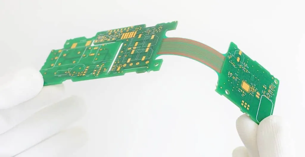
Semi-flex PCBs, also known as semi-rigid-flex boards, consist of a primarily rigid substrate with designated flexible regions created by thinning the material to approximately 0.2 to 0.4 mm. This construction uses standard FR4 laminates and prepregs, avoiding the polyimide films typical in full flexible or rigid-flex PCBs. The result is a board that supports surface-mount components on rigid areas while allowing controlled bending in flex tails or zones for 3D assembly. In industries like telecommunications and consumer electronics, semi-flex PCBs reduce assembly complexity by eliminating connectors between rigid and flex sections. They offer superior vibration resistance and thermal stability over pure flex boards, making them ideal for environments with dynamic mechanical loads. For electric engineers, understanding semi-flex PCB fabrication techniques ensures designs optimize space, weight, and reliability without escalating costs.
The relevance of semi-flex PCBs grows with miniaturization trends, as they bridge the gap between rigid and fully flexible solutions. Traditional rigid boards limit form factors in curved enclosures, while full flex circuits complicate component mounting and increase expense. Semi-flex manufacturing allows iterative thinning post-lamination, enabling prototypes to evolve into production-ready boards efficiently. Compliance with standards like IPC-2223 for flex design guidelines supports consistent performance across batches. Engineers benefit from shorter lead times and lower tooling costs, critical for high-volume projects.
Technical Principles Behind Semi-Flex PCBs
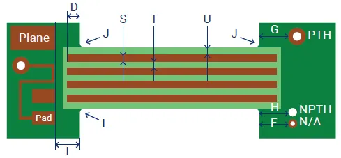
The core principle of semi-flex PCB manufacturing lies in selective material reduction to impart flexibility without compromising circuit integrity. FR4 materials with low-flow prepregs prevent resin bleed during thinning operations, ensuring uniform dielectric properties. Flex zones typically feature 1 or 2 copper layers to minimize stress concentrations during repeated bending. Mechanical properties depend on precise thickness control, as variations beyond tolerances lead to cracking or delamination under cyclic loads. Engineers must account for bend radius limits, often 10 times the flex zone thickness, to avoid fatigue failure. These principles align with IPC-2223 requirements for flex-to-install applications, guiding layer stackup and transition geometries.
Thinning alters the board's stiffness profile, creating hinge-like areas that absorb shocks better than monolithic rigid designs. Copper ductility in flex regions supports dynamic flexing, while rigid sections provide stable platforms for high-density interconnects. Thermal expansion mismatches between thinned and full-thickness areas require careful lamination pressure control to prevent warpage. Fabrication techniques like depth-controlled routing exploit FR4's machinability, contrasting with the chemical etching dominant in pure flex production.
The Semi-Flex PCB Manufacturing Process: Step-by-Step
The semi-flex PCB manufacturing process begins with design file preparation, specifying flex zone outlines and depth targets in Gerber or ODB++ formats. Material selection emphasizes thin FR4 cores (0.1 to 0.2 mm) and low-viscosity prepregs for multilayer builds. Panels undergo standard inner layer processing: photoresist application, exposure, development, etching, and stripping to define traces. Black oxide or alternative treatments enhance adhesion before layup. Lamination follows under vacuum pressure and controlled temperature ramps to fuse layers without voids. This stage sets the foundation for uniform thickness prior to flex zone creation.
Outer layer imaging and etching proceed similarly, defining pads, traces, and vias with high-resolution dry film or LDI processes. Drilling creates through-holes and blind vias using carbide or laser tools, followed by electroless copper seeding and electroplating for barrel integrity. Panel plating builds copper thickness to 18 or 35 microns, ensuring low-resistance interconnects. Solder mask application protects circuits, with legend printing for assembly aids. At this point, the semi-flex PCB fabrication techniques diverge with controlled depth milling.
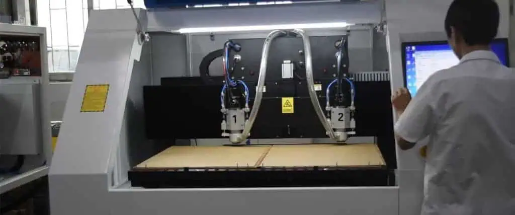
The pivotal step involves depth-controlled milling or laser ablation to thin flex zones precisely, targeting 0.25 mm nominal thickness. Mechanical routing uses high-speed spindles with depth sensors, while laser methods offer sub-micron accuracy for complex geometries. Operators program Z-axis stops to remove laminate and prepreg layers without exposing inner copper. Post-milling inspection verifies profile uniformity via optical profilometers. Final surface finishes like ENIG or HASL apply to pads, enhancing solderability. Electrical testing, including flying probe or bed-of-nails, confirms continuity and shorts before routing out individual boards.
Key Semi-Flex PCB Fabrication Techniques
Depth milling stands as the hallmark technique, employing carbide end mills with compression flutes to shear material cleanly. Parameters include feed rates of 1-2 m/min and spindle speeds over 50,000 RPM to minimize burrs and heat buildup. Laser ablation uses UV or CO2 lasers for non-contact thinning, ideal for fine-pitch flex tails where mechanical tools risk vibration damage. Both methods require fiducials for alignment, ensuring milled outlines match design tolerances within 0.1 mm. Hybrid approaches combine routing for bulk removal and laser finishing for edges.
Post-thinning, coverlay films occasionally apply to single-layer flex areas, though FR4 semi-flex often relies on thinned solder mask for protection. Sequential lamination techniques build asymmetric stackups, with flex zones starting as partial builds. Engineers optimize via-in-pad designs to avoid flex stress risers, favoring filled or staggered vias per IPC guidelines.
Essential Semi-Flex PCB Manufacturing Equipment
Core equipment includes multilayer lamination presses with vacuum capabilities for void-free bonds. Exposure units and etch lines handle high-resolution patterning, while vertical plating tanks deposit uniform copper. Depth milling demands CNC routers with optical height sensors and vibration-dampened tables for precision. Laser systems integrate galvo scanners for rapid ablation patterns. Automated optical inspection (AOI) stations scan for milling defects, complemented by X-ray for inner layer verification. Flying probe testers provide comprehensive netlist checks on finished boards.
Semi-Flex PCB Assembly Considerations
Assembly mirrors rigid PCB processes but incorporates flex supports to prevent zone deformation during reflow. Stencils align precisely, with solder paste inspection via SPI to avoid bridging in tight flex traces. Pick-and-place machines use low-force nozzles for delicate areas, followed by convection reflow ovens profiled for FR4 thermal limits. Post-reflow, flex zones undergo gentle cleaning to remove flux residues without abrasion. Manual bending occurs after full cure, respecting minimum radii to avoid trace fractures. J-STD-001 guidelines govern workmanship, emphasizing strain relief at rigid-flex transitions.
Semi-Flex PCB Quality Control Measures
Quality control spans in-process checks and final qualification per IPC-6013 for flexible printed boards. Microsectioning verifies milled depths and plating integrity, while warpage measurements use shadow moire interferometry. Bend cycle testing simulates 1,000 cycles at specified radii, monitoring resistance changes. Peel strength tests confirm adhesion in thinned regions, targeting 1.5 N/mm minimum. Electrical reliability includes high-voltage isolation and thermal cycling. Automated visual inspection detects cracks or delams early.
Visual and dimensional inspections ensure flex outlines match artwork, with tolerances under 0.15 mm. Moisture sensitivity handling follows JEDEC standards, baking boards pre-assembly to prevent popcorning.
Best Practices and Troubleshooting
Adhere to generous bend radii and teardrop pads to distribute stresses evenly. Simulate flex zones in design software for warpage prediction. Avoid vias in high-flex areas unless reinforced. Common issues like milling overcut stem from dull tools; mitigate with frequent edge inspections. Delamination in flex tails signals prepreg flow problems, resolved by lower lamination pressures. For warpage, balance stackups symmetrically where possible.
Conclusion
Mastering semi-flex PCB manufacturing empowers engineers to deliver compact, durable solutions through precise fabrication techniques and rigorous quality control. The step-by-step process, from lamination to depth milling, balances cost and performance effectively. Key to success lies in standards compliance, equipment calibration, and proactive troubleshooting. As demands for 3D electronics rise, semi-flex PCBs will remain a versatile choice for innovative designs.
FAQs
Q1: What is the semi-flex PCB manufacturing process?
A1: The semi-flex PCB manufacturing process follows standard rigid fabrication up to lamination, then incorporates depth-controlled milling or laser ablation to thin flex zones to 0.25 mm. Inner and outer layers pattern via imaging and etching, with drilling and plating for vias. Final steps include solder mask, surface finish, and testing. This factory-driven approach ensures reliable flex-rigid integration without polyimide lamination.
Q2: What are essential semi-flex PCB fabrication techniques?
A2: Key techniques include mechanical depth routing with CNC precision and laser ablation for non-contact thinning. Both maintain tight depth tolerances to create bendable areas from FR4 stock. Post-milling, AOI verifies uniformity. These methods offer cost advantages over rigid-flex while supporting multilayer designs.
Q3: How does semi-flex PCB quality control differ from rigid boards?
A3: Semi-flex PCB quality control adds bend testing, peel strength, and warpage checks per IPC-6013 alongside standard electrical and visual inspections. Flex zones undergo cycle fatigue simulations to confirm durability. Microsections validate thinning without delamination. This ensures performance in dynamic applications.
Q4: What equipment is critical for semi-flex PCB manufacturing?
A4: Critical equipment encompasses vacuum laminators, high-speed CNC routers for depth milling, laser ablation systems, and AOI scanners. Plating lines and flying probe testers complete the lineup. Precision tooling prevents defects in flex zones, supporting high yields.
References
IPC-2223 — Sectional Design Standard for Flexible Printed Boards. IPC
IPC-6013 — Qualification and Performance Specification for Flexible and Rigid-Flex Printed Boards. IPC
IPC-6012E — Qualification and Performance Specification for Rigid Printed Boards. IPC, 2017


