Introduction
In modern electronics design, fitting a printed circuit board (PCB) into its enclosure demands precise attention to dimensions to maximize available space and ensure reliable performance. Engineers face PCB enclosure size constraints that influence everything from thermal management to mechanical stability. Selecting the right standard PCB sizes guide helps balance functionality with manufacturability, avoiding costly redesigns or assembly issues. This guide explores compact PCB design principles, PCB component density considerations, and PCB miniaturization techniques tailored for electric engineers. By aligning PCB dimensions with enclosure requirements early in the process, designs achieve optimal space utilization and compliance with industry practices. Understanding these factors leads to more efficient prototypes and production-ready boards.
Understanding PCB Dimensions and Their Role in Enclosure Integration
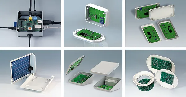
PCB dimensions encompass length, width, thickness, and outline tolerances, all critical for seamless enclosure integration. Standard PCB sizes do not follow rigid formats like paper sizes but align with common manufacturing panel dimensions, typically 18 by 24 inches or 12 by 18 inches, to optimize yield. These panel sizes dictate practical board dimensions, with usable areas around 16 by 22 inches after accounting for routing borders of 0.5 to 1 inch. Engineers must consider PCB enclosure size constraints, such as internal enclosure dimensions and mounting hole positions, to prevent interference. Thickness variations, commonly 0.8 mm, 1.57 mm, or 1.6 mm, also affect standoff heights and lid closure. Proper dimension selection ensures the board fits without excessive gaps that could lead to vibration issues or restricted airflow.
PCB Enclosure Size Constraints: Key Mechanical Considerations
Enclosure size constraints arise from the need for clearances around the PCB edges, components, and connectors to facilitate assembly and maintenance. A typical approach adds 5 to 10 mm margin beyond PCB dimensions for edge clearance, allowing tool access and thermal expansion. Component protrusions, such as capacitors or heatsinks, further dictate vertical space, often requiring 20 percent extra internal height for airflow. Mounting features like standoffs or card guides impose additional constraints, aligning with standard hole patterns for reproducibility. Tolerances play a pivotal role; board outlines typically hold to plus or minus 0.13 mm for precision fits. Addressing these constraints early prevents fitment failures during integration testing.
Navigating Standard PCB Sizes for Efficient Manufacturing
While individual PCBs are custom-sized, adhering to a standard PCB sizes guide based on panelization improves cost and lead times. Common single-board sizes derive from panel efficiencies, favoring multiples that tile neatly within 18 by 24 inch panels. For instance, boards up to 100 by 160 mm fit multiple times per panel, minimizing waste. Electric engineers should prioritize even multiples of routing grid sizes, often 0.1 mm increments, for depanelization accuracy. IPC-2221 provides generic guidelines for board design, including dimensioning practices that support panel utilization. Selecting sizes within these norms reduces handling risks during assembly and aligns with automated processes.
Balancing PCB Component Density with Enclosure Limits
PCB component density directly impacts enclosure sizing, as higher densities demand smaller footprints but complicate routing and heat dissipation. Engineers evaluate density by components per square inch, aiming for layouts that maintain signal integrity under space constraints. High-density areas near connectors require careful spacing to avoid shorts, while passive components cluster efficiently in low-signal zones. Compact PCB design involves zoning components by function, grouping high-power elements for better cooling access. Enclosure constraints limit maximum density; overly packed boards may exceed thermal budgets within tight volumes. Optimizing density ensures the PCB fits while preserving performance margins.
PCB Miniaturization Techniques for Space-Constrained Applications
PCB miniaturization techniques enable fitting complex circuitry into restrictive enclosures without sacrificing reliability. Techniques include finer pitch components, such as 0.4 mm BGA packages, and embedded passives to reclaim surface area. Multi-layer stackups increase density vertically, with 6 to 8 layers common for compact designs. Via-in-pad and blind vias reduce footprint sizes, though they raise fabrication complexity. IPC standards like IPC-6012E outline qualification for such high-density interconnects, ensuring warpage and registration tolerances meet enclosure demands. Engineers apply these methods iteratively, simulating fits to verify mechanical compatibility.
Practical Best Practices for Dimension Selection and Verification
Start dimension selection by defining enclosure internals first, then reverse-engineer PCB bounds with 10 percent lateral and 20 percent vertical buffers. Use mechanical CAD to overlay PCB outlines, checking interferences at maximum tolerances. Incorporate fiducials and tooling holes per IPC guidelines for precise panelization. For compact designs, prototype with rapid-turn panels to validate fits before full production. Simulate thermal profiles to confirm density choices do not overload enclosure ventilation. Document tolerances explicitly, targeting plus or minus 0.1 mm for outlines in high-volume runs. These practices streamline the path from schematic to housed assembly.
Troubleshooting Common Fit Issues in PCB-Enclosure Pairs
Fit issues often stem from overlooked tolerances or asymmetric component heights. Warpage, controlled under IPC-A-600 criteria, can misalign boards exceeding 0.75 percent bow. Engineers mitigate by specifying symmetric layer stackups and bow-resistant materials. Connector misalignment arises from cumulative tolerances; use adjustable slots or floating mounts. High component density exacerbates EMI shielding gaps; integrate gaskets early. Iterative mockups with 3D prints reveal issues before fabrication. Addressing these ensures robust, space-maximized assemblies.
Conclusion
Selecting the right standard PCB dimensions optimizes enclosure utilization, balancing PCB enclosure size constraints with performance needs. Key strategies include leveraging panel standards, managing component density, and applying miniaturization techniques judiciously. Adhering to guidelines from IPC-2221 and related documents ensures manufacturability and reliability. Electric engineers benefit from early integration planning, using clearances and tolerances to avoid pitfalls. This approach yields compact, efficient designs ready for production. Ultimately, precise dimensioning maximizes space while upholding engineering integrity.
FAQs
Q1: What are the main PCB enclosure size constraints to consider during design?
A1: PCB enclosure size constraints include edge clearances of 5 to 10 mm, component height allowances with 20 percent vertical buffer, and mounting hole alignments. Tolerances like plus or minus 0.13 mm on outlines prevent binding. Thermal vents and cable routing further limit internals. Engineers verify via 3D models to ensure compact PCB design fits seamlessly.
Q2: How does PCB component density affect standard PCB sizes guide choices?
A2: Higher PCB component density necessitates smaller boards but demands multi-layering for routing. A standard PCB sizes guide favors panels fitting multiple dense boards efficiently. Density impacts heat, requiring enclosure vents. Balance by zoning components logically to maintain signal quality within constraints.
Q3: What PCB miniaturization techniques help with tight enclosure fits?
A3: PCB miniaturization techniques like fine-pitch SMDs, embedded components, and HDI vias shrink footprints. Multi-layer boards up to 8 layers increase density without expanding area. IPC-6012E qualifies these for reliability. Simulate thermal and mechanical stresses to confirm enclosure compatibility.
Q4: Why reference IPC standards in PCB dimension selection?
A4: IPC standards provide factual guidelines for dimensions, tolerances, and qualifications under enclosure constraints. They ensure panelization efficiency and assembly repeatability. Consistent application avoids warpage and fit issues in compact designs.
References
IPC-2221B — Generic Standard on Printed Board Design. IPC, 2012
IPC-6012E — Qualification and Performance Specification for Rigid Printed Boards. IPC, 2017
IPC-A-600K — Acceptability of Printed Boards. IPC, 2020


