Introduction
High-frequency applications demand printed circuit boards that balance electrical performance with thermal reliability. Metal-backed PCBs emerge as a key solution in environments where signal speeds exceed gigahertz ranges and power dissipation challenges conventional designs. These boards integrate a solid metal substrate, typically copper or aluminum, beneath a dielectric layer and copper traces, enhancing both PCB performance and signal integrity PCB characteristics. Engineers face issues like electromagnetic interference and heat buildup that degrade high-speed PCB design outcomes. By providing a robust ground plane and efficient heat path, metal-backed PCB high frequency configurations address these concerns effectively. This article explores their principles, benefits, and implementation strategies aligned with factory production insights.
What Are Metal-Backed PCBs and Why Do They Matter for High-Frequency Use?
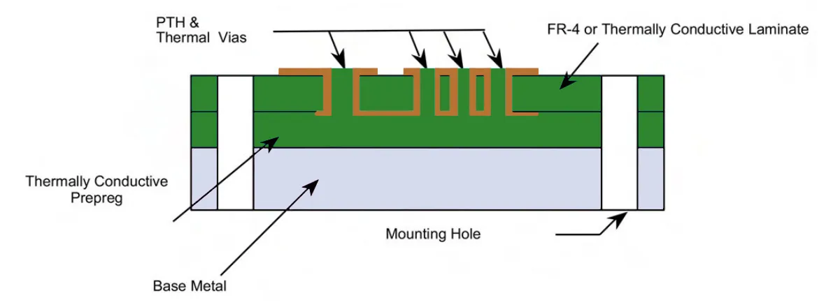
Metal-backed PCBs feature a metal core or backing directly bonded to a thin, thermally conductive dielectric and the top copper circuitry. Unlike standard FR-4 boards, this construction channels heat away from components, preventing hotspots that could warp traces or shift dielectric properties. In high-frequency contexts, such as RF amplifiers or microwave modules, components generate significant thermal loads alongside fast signal transitions. The metal layer serves dual purposes: superior thermal spreading and a low-impedance ground reference, critical for EMI shielding PCB effectiveness. Factory processes ensure the dielectric maintains low loss tangent values to minimize signal attenuation at frequencies above 1 GHz. Without such designs, standard boards suffer from increased insertion loss and crosstalk, compromising overall system reliability.
These boards matter because high-speed signals propagate as electromagnetic waves where even minor impedance discontinuities cause reflections. The continuous metal plane underneath offers a stable return path, reducing loop inductance that plagues multilayer stacks. Production aligns with standards like IPC-6018, which qualifies high-frequency boards including metal-backed variants for microwave performance. Dimensional stability from the metal substrate resists warpage during reflow or operation, preserving trace geometries essential for controlled impedance. In applications like radar systems or 5G base stations, this translates to consistent phase stability and lower bit error rates. Engineers select metal-backed options when thermal margins and signal fidelity coexist as primary requirements.
Technical Principles Behind Signal Integrity in Metal-Backed High-Frequency PCBs
Signal integrity in high-frequency PCBs hinges on controlling reflections, crosstalk, and losses influenced by material properties and geometry. At elevated frequencies, skin effect confines currents to trace surfaces, amplifying resistance and radiation tendencies. The metal backing acts as an extensive ground plane, shortening return current paths and minimizing inductance per IPC-2221 design guidelines for generic boards. This setup confines fields between traces and ground, akin to microstrip transmission lines with enhanced shielding. Dielectric materials with low dissipation factor, paired with the metal's high conductivity, preserve signal amplitude over distance. Factory lamination processes bond these layers under controlled pressure to avoid voids that could introduce parasitic capacitance.
EMI shielding PCB benefits arise from the metal layer blocking backside radiation and coupling to external fields. In high-power RF scenarios, amplifiers produce harmonics that standard boards radiate freely, violating emission limits. The solid backplane reflects these energies, converting them to heat that dissipates efficiently. Performance metrics improve as ground bounce diminishes, with via transitions to the backplane providing low-inductance stitching points. Simulations confirm eye diagram closure reduces by up to relevant margins in optimized stacks. Overall, these principles elevate PCB performance in dense, multi-layer high-speed PCB design environments.
Key Performance Enhancements from Metal-Backed Construction
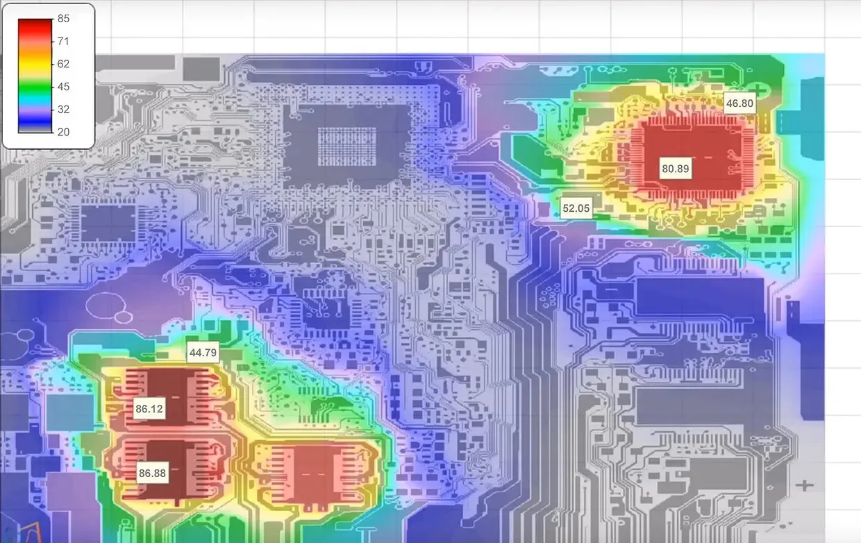
Metal-backed PCB high frequency designs excel in thermal management, directly impacting electrical reliability. Heat from power transistors spreads laterally across the metal, maintaining junction temperatures below critical thresholds. This stability prevents dielectric constant drift, which skews characteristic impedance at gigahertz bands. Signal integrity PCB metrics like return loss improve due to uniform substrate thickness post-fabrication. EMI shielding PCB layers inherently suppress cavity resonances that plague enclosed modules. Production verifies flatness to ensure consistent coupling factors across the board.
In high-speed PCB design, the metal plane supports embedded stripline routing with tighter field containment than air-exposed traces. Vias plated through the dielectric but insulated from the core maintain signal paths without shorting. Ground vias to the backing further suppress common-mode currents, enhancing noise immunity. Factory testing per IPC-6012 performance specs confirms these attributes through S-parameter measurements. Compared to cored laminates, metal-backed variants offer lower CTE mismatch risks when soldered. These enhancements make them ideal for phased-array antennas or mmWave transceivers.
Best Practices for Implementing Metal-Backed PCBs in High-Frequency Designs
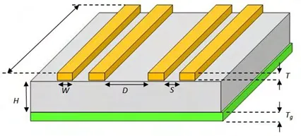
Select dielectrics with dielectric constant below 3.5 and loss tangent under 0.003 for minimal propagation delay variations. Stackup planning positions the metal back adjacent to the primary ground layer, optimizing via stub lengths. In high-speed PCB design, route critical nets as coupled microstrips over the backplane, maintaining 50-ohm impedance with width calculators. Avoid routing across core edges where mechanical stress concentrates. Factory guidelines recommend blind or filled vias for heat paths, preventing solder wicking issues. Ground stitching vias every quarter wavelength secure field containment.
Address EMI shielding PCB needs by integrating the metal back into chassis mounts with conductive epoxy. Simulate crosstalk budgets early, adjusting trace spacing to below 3:1 edge coupling rules. Thermal vias under hot components bridge to the backplane, sized per current density limits. Production panels include fiducials for precise alignment during lamination. Post-fabrication, X-ray inspections verify via integrity without core penetration. These practices ensure robust signal integrity PCB outcomes in volume manufacturing.
Common Challenges and Factory-Driven Solutions
Mechanical stress from CTE differences between metal, dielectric, and copper can induce microcracks during thermal cycling. Factory annealing steps relieve residual stresses post-lamination. Signal integrity degrades if ground isolation fails, so insulated buried vias use epoxy plugs. EMI leaks occur at board edges; beveled metal rims or gaskets mitigate this. Warpage control involves symmetric copper balancing opposite the core. Qualification follows IPC-6018 protocols for high-frequency endurance.
High-power density amplifies these issues, but metal spreading limits deltas to safe levels. Procurement specs detail backplane thickness, typically 1-2 mm for rigidity. Troubleshooting involves TDR scans for impedance steps at transitions. Solutions prioritize design-for-manufacturability from inception.
Conclusion
Metal-backed PCBs transform high-frequency applications by merging thermal resilience with superior signal handling. Their ground plane architecture bolsters EMI shielding PCB capabilities and PCB performance under demanding conditions. Adhering to best practices in stackup, routing, and production yields reliable high-speed PCB design results. Engineers gain predictable outcomes in RF and microwave realms. Future iterations will leverage thinner dielectrics for even higher frequencies. Selecting these boards elevates system margins effectively.
FAQs
Q1: What role does the metal backing play in signal integrity PCB for high-frequency signals?
A1: The metal backing provides a low-inductance ground plane, shortening return paths and reducing crosstalk in metal-backed PCB high frequency setups. It confines electromagnetic fields, minimizing radiation losses and reflections. Factory processes ensure smooth interfaces for consistent impedance. This enhances eye opening and jitter performance per design standards. Overall, it stabilizes signals in GHz environments.
Q2: How does EMI shielding PCB improve with metal-backed designs?
A2: Metal-backed constructions block backside emissions and external interference through the solid conductive plane. In high-speed PCB design, this lowers cavity modes and harmonic radiation from amplifiers. Ground stitching integrates the backplane fully, suppressing common-mode noise. Production verifies shielding effectiveness via near-field scans. Benefits include compliance with emission limits without added cans.
Q3: Why choose metal-backed PCB high frequency over standard laminates for performance?
A3: Standard boards warp under heat, shifting trace positions and degrading PCB performance. Metal backing offers dimensional stability and heat dissipation, preserving signal integrity PCB traits. It supports higher power densities in RF apps. Factory alignment ensures uniform dielectric thickness. This choice optimizes reliability for microwave modules.
Q4: What are key considerations in high-speed PCB design using metal-backed boards?
A4: Focus on via insulation to avoid core shorts and thermal vias for heat transfer. Maintain symmetric copper for flatness. Select low-loss dielectrics matching metal CTE. EMI shielding PCB integrates via edge fencing. Production follows qualification specs for endurance.
References
IPC-6018D — Qualification and Performance Specification for High Frequency (Microwave) Printed Boards. IPC, 2022
IPC-2221 — Generic Standard on Printed Board Design. IPC, 2012
IPC-6012E — Qualification and Performance Specification for Rigid Printed Boards. IPC, 2017


