Introduction
Optimizing PCB layout for energy efficiency has become essential in modern electronics design, where devices must operate longer on limited power sources. Electrical engineers face increasing pressure to create systems that minimize energy waste, particularly in battery-powered applications like wearables, sensors, and edge computing nodes. PCB layout energy efficiency directly influences resistive losses, switching inefficiencies, and thermal overhead, all of which contribute to higher overall power consumption. Effective layouts reduce voltage drops, limit parasitic inductance, and improve heat spreading, leading to cooler operation and extended device lifespan. As sustainability goals drive the industry toward greener practices, mastering these techniques ensures compliance with performance demands while lowering environmental impact. This article details structured approaches to low power PCB layout and thermal management PCB design.
Why PCB Layout Energy Efficiency Matters
Energy-efficient PCB layouts matter because they address core challenges in power delivery and dissipation across electronic systems. In high-density boards, inefficient routing amplifies I-squared-R losses, forcing regulators to compensate with higher input power and generating excess heat. This not only shortens battery life in portable devices but also raises operational costs in data centers and industrial controls. Thermal management PCB design plays a pivotal role, as unmanaged heat leads to derating components and requiring active cooling, which consumes additional energy. From an environmental perspective, green PCB design techniques reduce material use in cooling solutions and lower carbon footprints through prolonged product lifecycles. Engineers prioritizing these aspects align with broader industry shifts toward net-zero emissions.
Beyond performance, energy optimization enhances signal integrity by stabilizing supply rails, reducing noise that could trigger protective shutdowns. In applications like renewable energy inverters, even small efficiency gains compound into substantial savings over time. Layout decisions early in the design cycle prevent costly respins and ensure scalability for future iterations. Ultimately, PCB layout energy efficiency bridges functionality, reliability, and sustainability in engineering practice.
Fundamental Principles of Energy-Efficient PCB Layout
The principles underlying energy-efficient PCB layouts revolve around minimizing electrical and thermal resistances throughout the board. Power distribution networks must deliver current with minimal voltage sag, achieved by favoring wide conductors and solid planes over serpentine traces. Parasitic effects, such as loop inductance in ground returns, induce voltage spikes that inefficiently draw quiescent current from supplies. Thermal principles dictate that heat from power devices flows efficiently to ambient via copper features and vias, preventing hotspots that accelerate aging. Balancing these factors requires understanding current density limits to avoid excessive temperature rises.
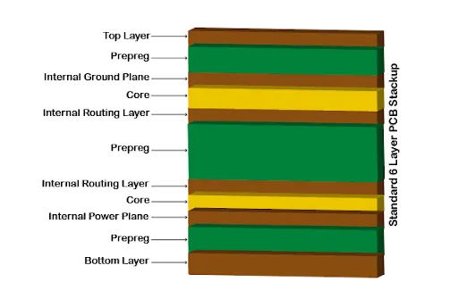
Resistance in traces follows Ohm's law, where narrower paths increase drops and losses under load. Inductance arises from current loop areas, particularly in switching circuits, leading to ringing and higher peak currents. Capacitive coupling between layers adds leakage paths, subtly elevating standby power. Effective layouts integrate these considerations holistically, using multilayer stackups to separate noisy power from sensitive signals. Adhering to guidelines in IPC-2221C ensures robust designs that inherently support low power operation.
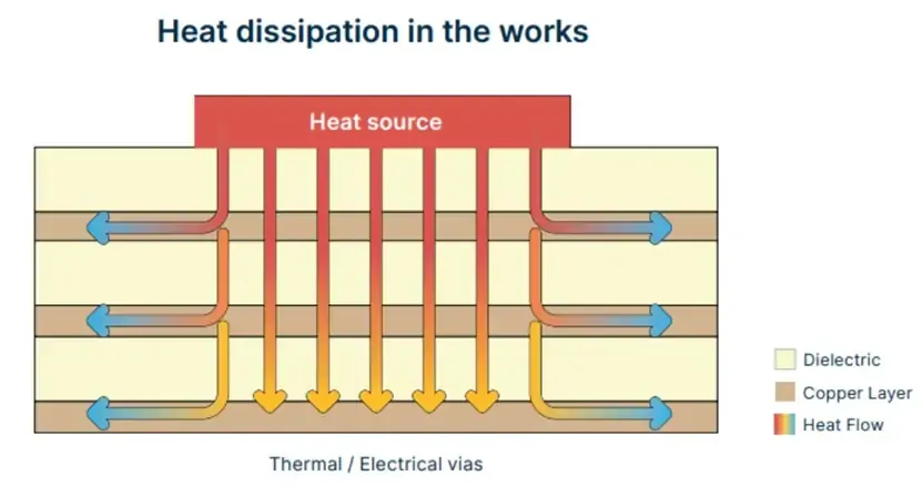
Heat generation ties directly to power dissipation, where I2R losses convert electrical energy to thermal. Conduction through copper dominates in-plane spreading, while vias bridge layers for vertical paths. Convection and radiation become relevant at board edges, but layout must first maximize internal dissipation. Engineers model these paths iteratively to predict efficiency before fabrication.
Practical Techniques for Reducing Power Consumption in PCB Design
Reducing power consumption PCB starts with strategic component placement to localize currents and heat. Position high-current elements near board edges or mounting points for direct chassis coupling, minimizing long traces that waste energy. Group analog and digital sections separately to prevent noise-induced retries, which spike dynamic power. Place voltage regulators adjacent to loads, using short, wide paths to cut distribution losses. This zoning reduces crosstalk and enables tailored ground planes.
Power planes form the backbone of low power PCB layout by providing near-zero resistance distribution. Dedicate inner layers to solid Vcc and GND pours, stitching them with dense vias to equalize potentials. Split planes only where voltage domains differ, using jumpers or moats to isolate without creating slots that increase inductance. For multilayer boards, alternate signal and plane layers to shield and contain fields, further curbing emissions that demand compensatory drive power.
Trace routing demands wider dimensions for DC power nets, sized according to IPC-2152 to limit temperature rise below 20 degrees Celsius. Employ 45-degree bends over 90-degree to reduce reflections in high-speed signals, indirectly saving power through cleaner edges. Minimize vias in critical paths, as each adds resistance and inductance; array them in parallel where necessary. Signal return paths should mirror sources closely, shrinking loop areas and EMI that triggers shielding overhead.
Decoupling capacitors must sit within millimeters of IC power pins to suppress transients without reservoir discharge. Use multiple values in parallel, ceramic for high-frequency and tantalum for bulk, to cover spectra efficiently. Place them under ICs on opposite layers if space constrains, connected via short vias. This setup stabilizes rails, preventing brownouts that inefficiently reset systems.
Thermal management PCB design integrates vias arrays under hot components, acting as heat pipes to inner planes. Fill unused areas with copper pours tied to GND, boosting effective thermal conductivity. For high-power LEDs or FETs, route thermal pads directly to planes without signal interruptions. These features dissipate heat passively, eliminating fans and their power draw.
Green PCB design techniques extend to layer count optimization; thinner stackups with embedded planes reduce via lengths and capacitance. Avoid unnecessary splits that fragment pours, increasing edge effects. Simulate power integrity early to verify drops stay under 5% of supply.
Advanced Strategies in Thermal Management and Low-Power Optimization
Advanced thermal management PCB design leverages via tents and filled vias for multilayer heat transfer without compromising insulation. Stagger via grids to maximize density while respecting drill limits, channeling heat to outer layers or heatsinks. Copper-balanced pours equalize CTE mismatches, preventing warpage that contacts components inefficiently.
In low power scenarios, star-point grounding converges returns at a single low-inductance node, avoiding ground bounce across domains. Ferrite beads on power entries filter noise without broad resistive drops. Dynamic power gating isolates idle sections via MOSFETs, their gates driven minimally.
Stackup planning assigns thicker copper to power layers for lower resistance, tapering signals finer. IPC-6012 specifications guide qualification, ensuring thermal performance post-fabrication. These layered approaches yield boards where efficiency exceeds 95% in delivery.
Conclusion
Optimizing PCB layout for energy efficiency demands a systematic integration of electrical and thermal principles. Techniques like solid planes, precise trace sizing per IPC-2152, and strategic decoupling directly cut losses and heat. Electrical engineers benefit from these green PCB design techniques by delivering reliable, sustainable products. Prioritizing layout early yields compounding gains in power savings and environmental stewardship. Future designs will lean heavier on simulation-driven refinements, pushing efficiency boundaries further.
FAQs
Q1: How does PCB layout energy efficiency impact battery life in IoT devices?
A1: Efficient layouts minimize resistive drops and parasitics, ensuring stable supplies that reduce regulator overhead. Thermal management PCB design prevents throttling, allowing full-speed operation longer. Short power paths and planes lower quiescent draw, extending runtime by optimizing every microamp. Overall, these yield significant gains without component changes.
Q2: What are key steps for reducing power consumption PCB through routing?
A2: Start with wide traces per current needs, favoring planes for distribution. Minimize loop areas and vias in high-current nets to cut inductance losses. Separate noisy paths from quiet ones, reducing EMI mitigation power. Stitch planes densely for equipotential grounds. Verify with power integrity analysis before and during layout.
Q3: Why is thermal management PCB design crucial for low power PCB layout?
A3: Heat from losses demands cooling energy, and efficient dissipation via vias and pours avoids this. Hotspots degrade efficiency via leakage currents. Proper placement spreads load, stabilizing performance. It enables passive cooling, aligning with green goals. Standards like IPC-2221C guide reliable implementation.
Q4: What green PCB design techniques enhance overall energy efficiency?
A4: Use multilayer planes for low-resistance delivery and thermal vias for passive cooling. Optimize stackups to shorten paths, minimizing capacitance. Balanced copper reduces warpage risks. Decoupling near loads cuts transients. These techniques holistically lower system draw and material needs.
References
IPC-2221C - Generic Standard on Printed Board Design. IPC, 2023
IPC-2152 - Standard for Determining Current Carrying Capacity in Printed Board Traces. IPC, 2009
IPC-6012DS - Qualification and Performance Specification for Rigid Printed Boards. IPC, 2020


