Introduction
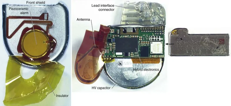
Pacemaker PCBs represent the core of life-sustaining implantable devices, where power management directly influences operational longevity and patient safety. These boards integrate sensing circuits, pulse generators, telemetry systems, and control logic within a hermetically sealed enclosure powered by primary batteries that cannot be easily replaced. Efficient battery usage becomes critical as pacemakers must function reliably for over a decade without intervention. Low-power PCB design for pacemakers focuses on minimizing quiescent currents, dynamic power draw during pacing, and standby losses to extend service life. This article explores strategies for pacemaker PCB power consumption optimization, drawing on engineering principles to achieve battery life extension in medical implants. By addressing PCB-level challenges, engineers can enhance overall system reliability.
Why Power Management Matters in Pacemaker PCBs
Pacemakers operate in a constrained environment where battery capacity is limited to small lithium-based cells, typically offering finite energy before depletion necessitates surgical replacement. Power mismanagement accelerates battery drain, risking device failure and endangering patients dependent on continuous cardiac support. In PCB design, inefficiencies such as parasitic losses or suboptimal routing amplify consumption, shortening implant lifespan. Optimizing power at the PCB level aligns with the demand for longer intervals between procedures, reducing healthcare costs and patient risks. Key metrics include average current draw below microampere levels during sensing and efficient energy delivery for pacing pulses. Ultimately, robust power management ensures compliance with high-reliability requirements for medical implants.
Core Technical Principles of Power Consumption in Pacemaker PCBs
Power in pacemaker PCBs originates primarily from non-rechargeable batteries, with consumption divided into sensing, pacing, communication, and housekeeping functions. Sensing circuits monitor cardiac signals with minimal bias currents, while pacing delivers controlled voltage pulses to the heart, demanding short bursts of high current. Telemetry for data transmission represents a significant draw, often managed through low-duty-cycle bursts. PCB contributions to power loss include dielectric absorption in substrates, conductor resistance in traces, and capacitive coupling between layers. Leakage currents through unclean interfaces or imperfect insulation further erode efficiency. Understanding these mechanisms allows engineers to target interventions for overall reduction.
Material selection plays a pivotal role, as substrates with low dissipation factors minimize energy loss during signal propagation. Thinner dielectrics reduce parasitic capacitance but increase field strength, necessitating careful stackup design. Component placement affects power distribution; grouping high-current paths shortens traces and lowers IR drops. Thermal management prevents efficiency degradation from self-heating in dense layouts. Ground plane integrity suppresses noise that could trigger unnecessary circuit activity, indirectly saving power. These principles form the foundation for low-power PCB design for pacemakers.
Mechanisms of Power Loss and Their PCB Implications
Dynamic power dominates during active states like pacing, governed by switching frequencies and load capacitance on the PCB. Static leakage arises from subthreshold currents in semiconductors and reverse-biased junctions, exacerbated by higher temperatures within the implant. PCB routing introduces series resistance, causing voltage droops that force regulators to compensate with excess dissipation. Vias and transitions between layers add inductance, ringing signals and increasing switching losses. Electromagnetic interference from adjacent traces induces currents, amplifying consumption. Quantifying these via simulation precedes physical optimization.
In standby mode, the PCB must enable ultra-low quiescent operation, where even nanoampere leaks matter over years. Solder joints and vias prone to electromigration degrade over time, raising resistance and power needs. Moisture ingress, though mitigated by encapsulation, alters dielectric properties if seals fail. Adherence to IPC-A-610 standards ensures assembly quality that preserves low-leakage paths. Vibration from cardiac motion stresses connections, potentially increasing contact resistance. Engineers must model cumulative effects for long-term projections.
Practical Solutions for Power Optimization
Power management ICs for pacemaker PCBs centralize regulation, offering buck-boost conversion with high efficiency and low quiescent draw. These ICs integrate sleep modes, dynamically scaling voltage to match load demands during sensing versus pacing. Duty cycling telemetry reduces average power by transmitting only essential data periodically. On the PCB, dedicated power planes segregate analog and digital domains, minimizing noise-induced retries. Decoupling capacitors placed proximate to IC pins stabilize rails, preventing overshoot losses.
Component selection emphasizes ultra-low-power op-amps and comparators for sensing, with CMOS processes favoring subthreshold operation. PCB layout prioritizes wide traces for pacing currents, star grounding to avoid loops, and guarded traces for sensitive nodes. Vias-in-pad techniques in HDI boards shorten paths, cutting resistance. Controlled impedance matching on high-speed telemetry lines preserves signal integrity without excess drive power. Fabrication per IPC-6012DS guidelines ensures minimal voids in plating, sustaining low resistance.
Energy harvesting for pacemakers supplements batteries, capturing mechanical energy from heartbeats via piezoelectric elements or blood flow vibrations. These transducers generate microwatts, rectified and stored in capacitors for peak loads. PCB integration requires flexible substrates to withstand flexing, with rectifiers and regulators occupying minimal area. Thermal harvesting from body heat uses thermoelectric generators, though output is low. RF scavenging from external fields provides intermittent boosts during clinic visits. Hybrid approaches combine sources for redundancy, extending effective battery life.
Battery life extension in medical implants involves adaptive algorithms that adjust pacing amplitude based on sensed thresholds, conserving energy during stable rhythms. Voltage monitoring circuits predict end-of-life, enabling elective replacements. PCB design supports this with precision references and ADCs drawing negligible power. Shielding cans around oscillators prevent EMI pulling higher currents. Testing under accelerated life conditions verifies optimizations.
Best Practices in Low-Power PCB Design for Pacemakers
Start with schematic-level power budgeting, allocating envelopes for each block and selecting components within them. Simulate transient responses to capture pacing peaks without undershoot. Stackup design favors symmetric builds for warpage control, using low-Dk materials like PTFE blends. Routing follows length-matched pairs for differentials, with stitching vias tying grounds. Solder mask over power traces reduces creepage risks in humid body environments.
Assembly demands Class 3 conformance per IPC-A-610, with X-ray inspection for hidden voids. Conformal coatings enhance insulation resistance, curbing leakage. Firmware implements event-driven processing over polling, slashing MCU activity. Over-the-air updates, when feasible, refine power profiles post-implant. Validation includes burn-in testing to weed out early failures.
Troubleshooting Common Power Issues
Excessive drain often traces to ground bounce; mitigate with multi-point grounding and ferrite beads. Telemetry overruns signal layout crosstalk; add shielding and filtering. Battery droop under load points to insufficient decoupling; audit cap values and ESR. Long-term drift suggests electromigration; upsize conductors per IPC-6012DS. Oscillator instability draws excess current; isolate and dampen. Systematic logging during bench testing isolates culprits.
Conclusion
Optimizing power management in pacemaker PCBs demands holistic attention from component selection through layout and assembly. Techniques like efficient PMICs, strategic routing, and emerging energy harvesting collectively enable battery life extension in medical implants. Adhering to standards ensures reliability under physiological stresses. Engineers achieve pacemaker PCB power consumption optimization by balancing miniaturization with efficiency. These practices not only prolong device service but also advance implantable technology safety.
FAQs
Q1: What are key strategies in low-power PCB design for pacemakers?
A1: Low-power PCB design for pacemakers emphasizes minimal quiescent currents through sleep modes, low-loss materials, and optimized routing to reduce parasitics. Power planes segregate domains, while HDI minimizes trace lengths. Energy-efficient components and duty cycling further cut average draw. This approach targets decade-long operation on primary batteries.
Q2: How does pacemaker PCB power consumption optimization extend battery life?
A2: Pacemaker PCB power consumption optimization involves leakage reduction via clean assembly and guarded traces, plus dynamic voltage scaling. Telemetry bursts replace continuous monitoring, saving energy. PCB-level simulations predict losses, guiding refinements. Resulting efficiency supports battery life extension in medical implants without size penalties.
Q3: Can energy harvesting for pacemakers replace batteries entirely?
A3: Energy harvesting for pacemakers, such as piezoelectric from cardiac motion, supplements rather than replaces batteries due to low output levels. PCB-integrated harvesters charge capacitors for peaks, extending runtime. Challenges include biocompatibility and variable harvest rates. Hybrid systems provide reliability margins.
Q4: What role do power management ICs play in pacemaker PCBs?
A4: Power management ICs for pacemaker PCBs handle regulation with high step-down efficiency and nanoampere sleep currents. They enable adaptive supply rails matching pacing needs. PCB placement near loads cuts distribution losses. Integration streamlines design while upholding IEC 60601 safety.
References
IPC-A-610 — Acceptability of Electronic Assemblies. IPC.
IPC-6012DS — Qualification and Performance Specification for Rigid Printed Boards (High Density Interconnect). IPC.
IEC 60601-1 — Medical electrical equipment - Part 1: General requirements for basic safety and essential performance. IEC.


