Introduction
Pacemakers represent one of the most demanding applications for printed circuit board design due to their role in sustaining human life through precise electrical stimulation of the heart. Signal integrity in pacemaker PCBs ensures that low-level sensing signals and pacing pulses remain undistorted amidst a challenging environment filled with biological noise and potential external interference. Any degradation in these signals can lead to device malfunction, such as inappropriate inhibition or unintended shocks, underscoring the need for meticulous design practices. Engineers must prioritize noise reduction in medical PCBs to maintain reliability over the device's multi-year lifespan. This article delves into key strategies for achieving robust signal integrity, focusing on impedance control, routing techniques, and electromagnetic compatibility measures. By adhering to established engineering principles, designers can mitigate risks inherent to these compact, high-stakes assemblies.
Understanding Signal Integrity in Pacemaker PCBs
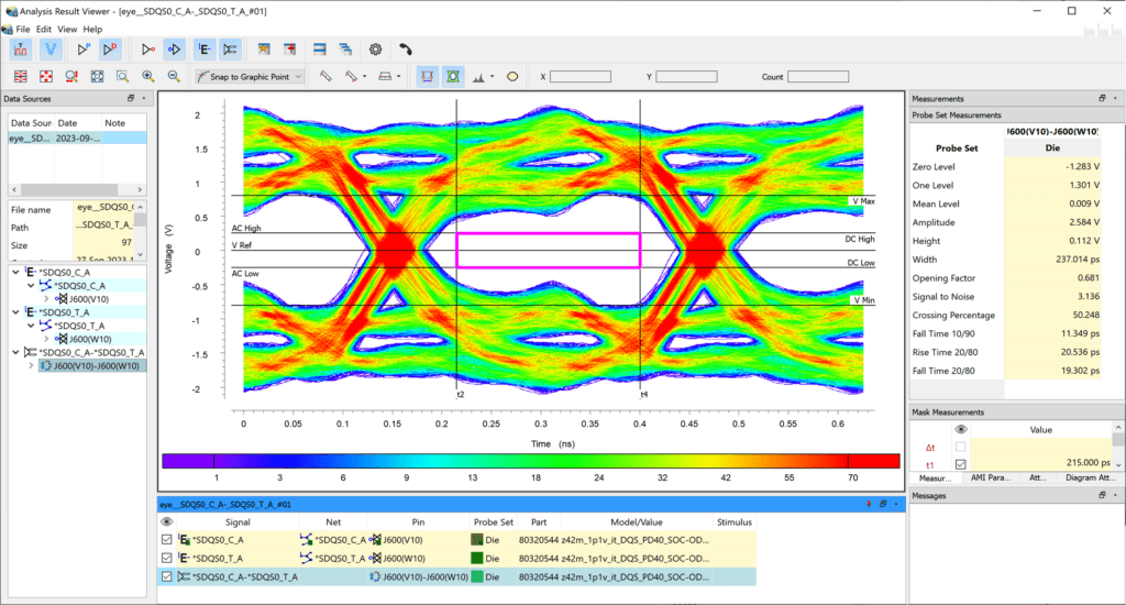
Signal integrity refers to the preservation of electrical signal quality from source to destination, encompassing aspects like waveform shape, timing, and amplitude fidelity. In pacemaker PCBs, this is particularly critical because the circuits handle microvolt-level signals from cardiac activity while generating precise millivolt pulses for stimulation. Noise sources, including crosstalk between traces, ground bounce, and electromagnetic interference from the body or external fields, can corrupt these signals, leading to erroneous detection or pacing failures. Pacemaker PCB impedance control becomes essential to prevent reflections that distort waveforms, especially in high-density layouts with fine-pitch components. Engineers must consider the interplay of dielectric materials, trace geometry, and layer stackup to maintain consistent characteristic impedance. Ultimately, robust signal integrity safeguards patient safety and device performance in implantable applications.
Pacemakers operate in a noisy physiological environment where muscle artifacts and electromagnetic fields from nearby tissues introduce interference. Medical device regulations demand that PCBs achieve high levels of noise reduction in medical PCBs through systematic design verification. Failure to address these challenges can result in compliance issues or field failures, emphasizing proactive engineering from the schematic stage. Structured analysis tools help quantify potential degradations early, allowing iterative improvements before fabrication.
Key Noise Sources and Interference Mechanisms in Pacemaker Designs
Noise in pacemaker PCBs arises primarily from electromagnetic coupling, where adjacent traces induce unwanted voltages via capacitive or inductive mechanisms. Crosstalk occurs when fast-switching signals on one trace couple to a victim trace, degrading signal-to-noise ratios critical for heart rhythm detection. Reflections from impedance discontinuities, such as abrupt width changes or unmatched vias, further exacerbate distortion by creating ringing on the line. Power supply noise propagates through ground planes if return paths lack low-impedance connections, coupling into sensitive analog sections. External electromagnetic interference penetrates enclosures, necessitating shielding strategies aligned with EMC compliance for pacemaker PCBs.
Thermal and mechanical stresses in implantable devices can shift material properties, altering impedance over time and introducing additional noise paths. Biological fluids introduce conductive paths that act as antennas for low-frequency interference. Engineers must model these effects using field solvers to predict coupling levels accurately. Understanding these mechanisms guides targeted mitigation during layout.
Principles of Impedance Control for Pacemaker Signals
Characteristic impedance in pacemaker PCB impedance control is governed by the ratio of inductance to capacitance per unit length in transmission lines formed by traces and reference planes. Maintaining a target impedance, typically 50 or 100 ohms for differential pairs, requires precise control of trace width, spacing, and dielectric thickness. Microstrip configurations expose traces to air, increasing effective dielectric constant variability, while striplines embedded between planes offer better stability but demand symmetric stackups. Variations beyond 10 percent tolerance can cause significant return loss, impacting signal quality. Layer stackup design must balance these parameters with routing density constraints inherent to miniature pacemaker boards.
Material selection influences loss tangent and propagation delay, both critical for low-jitter timing in pacing circuits. Achieving pacemaker PCB impedance control aligns with guidelines in IPC-2221C, which provides foundational principles for printed board design including conductor sizing and spacing. Simulations validate designs by predicting eye diagrams under worst-case conditions. Fabrication tolerances necessitate statistical process control to ensure repeatability.

Signal Routing Techniques for Pacemakers
Signal routing techniques for pacemakers emphasize minimizing loop areas and ensuring matched lengths for differential signals to suppress common-mode noise. Orthogonal routing between layers reduces broadside coupling, while dedicated ground reference planes adjacent to signal layers provide return paths that confine fields. Vias introduce stubs that reflect energy unless back-drilled or tuned with stubs. Length-matched routing prevents skew in clock or data lines, preserving timing margins. Avoiding right-angle bends in favor of 45-degree mitered corners reduces reflections and radiation.
Separation of analog and digital sections via ground stitching prevents noise migration, with guard traces shielding sensitive lines. Power distribution networks require decoupling capacitors placed strategically to bypass high-frequency noise. These practices form the core of noise reduction in medical PCBs. Pre-layout planning with constraint managers enforces rules systematically.
Grounding and Power Integrity Strategies
Effective grounding in pacemaker PCBs involves solid planes that minimize impedance at high frequencies, serving as low-inductance returns for all signals. Split planes for analog and digital domains require careful stitching with vias to avoid slots that radiate or couple noise. Star-point grounding consolidates returns at a single node for DC paths, preventing circulating currents. Decoupling schemes place capacitors close to IC pins, forming LC filters that shunt noise to ground.
Power integrity complements this by ensuring stable supply voltages free from ripple, using multi-layer planes for distribution. Ferrite beads and pi-filters attenuate conducted emissions. These measures support overall EMC compliance for pacemaker PCBs as outlined in IEC 60601-1-2:2014+A1:2020, which specifies immunity and emission limits for medical equipment.
Achieving EMC Compliance in Pacemaker PCB Design
Electromagnetic compatibility ensures pacemakers function without generating or succumbing to interference in clinical settings. Enclosure shielding with conductive gaskets blocks external fields, while internal partitions compartmentalize noisy sections. Filtered connectors prevent radiated emissions from escaping via cabling. Board-level shielding cans over RF-sensitive areas contain fields effectively.
Pre-compliance testing verifies margins against immunity levels like electrostatic discharge and radiated susceptibility. Layout symmetry and balanced routing reduce unintentional antennas. Adhering to high-reliability classes under IPC-6012F guarantees workmanship that supports long-term EMC performance. Iterative design-review cycles integrate these elements seamlessly.
Best Practices for Fabrication and Assembly
Fabrication processes must maintain tight tolerances on trace etch and plating to preserve impedance profiles. Supplier qualification ensures materials meet low-loss specifications suitable for medical use. Assembly introduces risks like solder voids that alter parasitics, necessitating X-ray inspection. Bake-out procedures mitigate moisture-induced failures in humid implant environments.
Design for testability includes probes for signal integrity verification post-assembly. Traceability from design to lot supports failure analysis. These steps embed quality from inception.
Conclusion
Signal integrity in pacemaker PCBs demands a holistic approach integrating impedance control, precise routing, robust grounding, and EMC strategies to minimize noise and interference. Engineers achieve this through structured adherence to principles that preserve signal fidelity in demanding implantable conditions. Key takeaways include prioritizing controlled impedance traces, layered shielding, and compliance-driven layouts. Implementing these practices not only enhances reliability but also streamlines regulatory approval. Pacemaker designers must continually refine techniques to meet evolving performance needs in medical electronics.
FAQs
Q1: What role does pacemaker PCB impedance control play in signal integrity?
A1: Pacemaker PCB impedance control maintains consistent characteristic impedance along signal paths, preventing reflections that distort low-amplitude cardiac signals. Proper trace geometry and stackup design ensure matched transmission lines, reducing ringing and overshoot. This technique aligns with design standards to support reliable pacing and sensing functions. Engineers verify control through time-domain reflectometry during validation.
Q2: How can noise reduction in medical PCBs be achieved through routing?
A2: Noise reduction in medical PCBs relies on signal routing techniques for pacemakers like increased spacing, length matching, and reference plane adjacency to minimize crosstalk and inductive coupling. Orthogonal layer routing and via shielding further isolate signals. Guard traces and ground stitching complete the strategy, preserving signal-to-noise ratios essential for precision diagnostics.
Q3: Why is EMC compliance critical for pacemaker PCBs?
A3: EMC compliance for pacemaker PCBs prevents susceptibility to external fields like MRI or ESD, which could inhibit therapy delivery. It involves shielding, filtering, and layout optimization to meet emission and immunity thresholds. Compliance ensures uninterrupted operation in diverse environments, safeguarding patient outcomes through verified robustness.
Q4: What are common signal routing techniques for pacemakers to minimize interference?
A4: Signal routing techniques for pacemakers include differential pairs with tight coupling, minimized vias, and symmetric returns to suppress common-mode noise. Avoiding high-current paths near sensors and using mitered bends reduce emissions. These methods enhance overall signal integrity while fitting compact form factors.
References
IPC-2221C — Generic Standard on Printed Board Design. IPC, 2023
IPC-6012F — Qualification and Performance Specification for Rigid Printed Boards. IPC, 2023
IEC 60601-1-2:2014+A1:2020 — Medical electrical equipment — Part 1-2: General requirements for basic safety and essential performance — Collateral Standard: Electromagnetic disturbances. IEC, 2020


