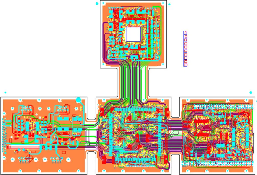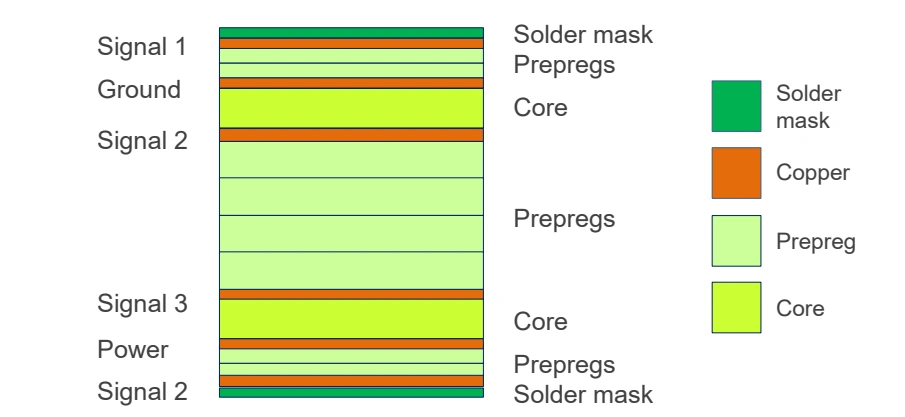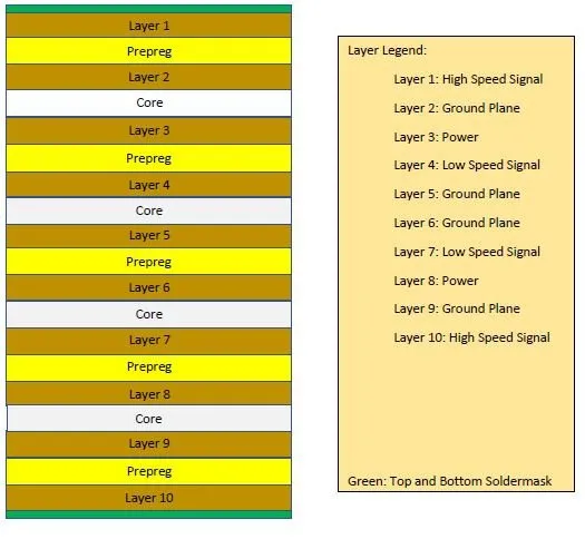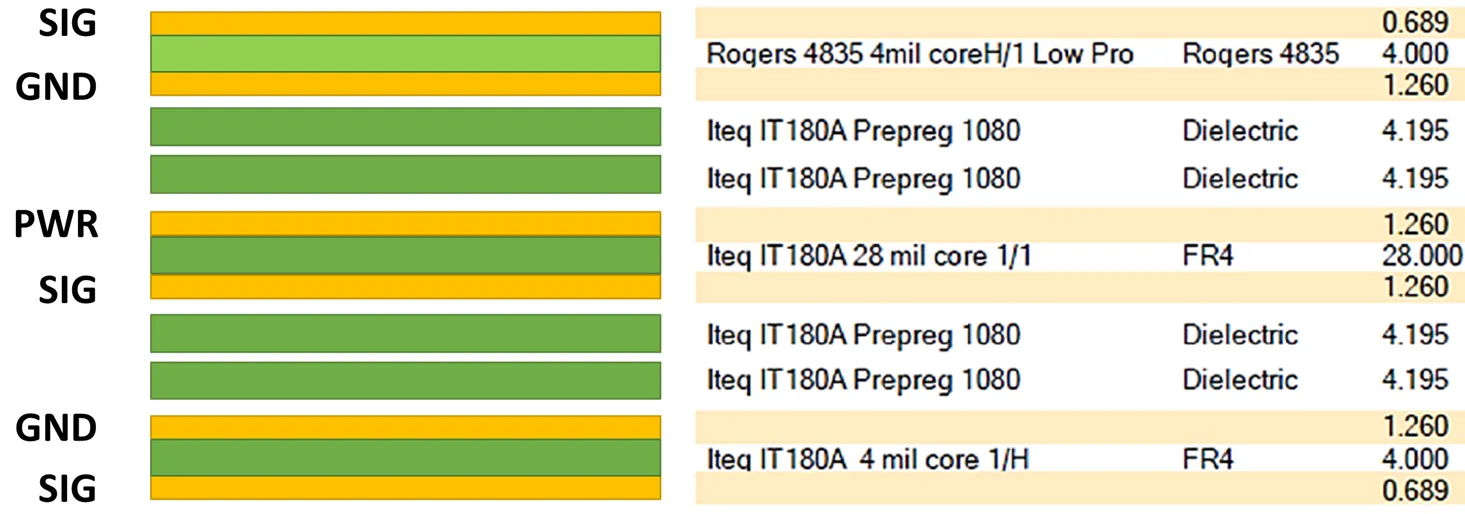
High Layer Count PCB Stackup Design for RF Applications: Minimizing Signal Loss
Cut PCB signal loss in high layer count RF PCB designs with proven stackup strategies and high frequency PCB materials. Covers dielectric losses, ground plane placement, symmetric layering, via optimization, and verification for reliable RF performance in dense boards.