Introduction
PCB panelization involves arranging multiple individual circuit boards onto a larger carrier panel to streamline fabrication and assembly processes. This technique directly impacts PCB manufacturing efficiency by reducing material waste and handling time during production runs. Electrical engineers often face challenges when designing irregular PCB shapes that complicate array layouts and increase costs. Optimizing PCB shapes for panelization ensures higher yields and compatibility with standard manufacturing equipment. Factory-driven insights emphasize aligning designs with proven practices to avoid depaneling defects and warpage issues. Understanding these principles allows teams to achieve cost-effective PCB manufacturing shapes without compromising performance.
What Is PCB Shape Panelization and Why It Matters
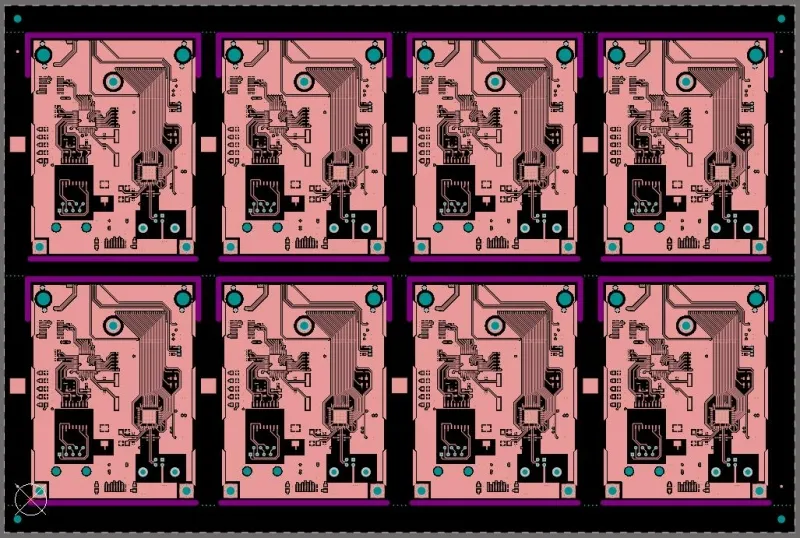
PCB shape panelization refers to the strategic grouping of single or multiple PCB designs into a unified panel, tailored to the board's outline for batch processing. This method enhances PCB manufacturing efficiency by enabling automated handling in etching, plating, and soldering stages. Irregular shapes demand custom spacing and support structures, leading to underutilized panel real estate and higher per-unit costs. Rectangular or near-rectangular forms allow tighter nesting, maximizing the number of boards per panel and minimizing scrap. In high-volume production, poor panel design can cause misalignment during fiducial recognition or stress concentrations during separation. Adhering to established guidelines ensures panels meet quality benchmarks, supporting reliable signal integrity and mechanical stability.
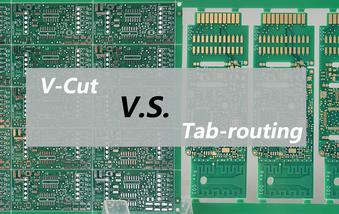
The relevance extends to assembly lines where panels reduce setup times between runs. Engineers must consider depaneling methods early, as they dictate shape constraints and edge clearances. V-scoring suits linear separations on straight-edged panels, while tab routing accommodates complex contours. Effective PCB panel design balances these factors to lower overall production expenses. Factories prioritize designs that fit standard panel dimensions without custom tooling, preserving throughput rates. Ultimately, thoughtful panelization transforms potential puzzles into predictable manufacturing advantages.
Technical Principles Behind PCB Array Optimization
The core principle of PCB array optimization revolves around material utilization and mechanical integrity during processing. Panels must provide uniform support to prevent warpage from thermal cycles in lamination and reflow soldering. Shape irregularities amplify bowing risks, as uneven copper distribution or asymmetric layer stacks induce stresses. Standards like IPC-6012E outline qualification criteria for rigid boards, including bow and twist limits that panels must respect to avoid assembly failures. Optimizing orientations, such as mirroring boards or rotating them at 90 degrees, fits more units while distributing thermal loads evenly.
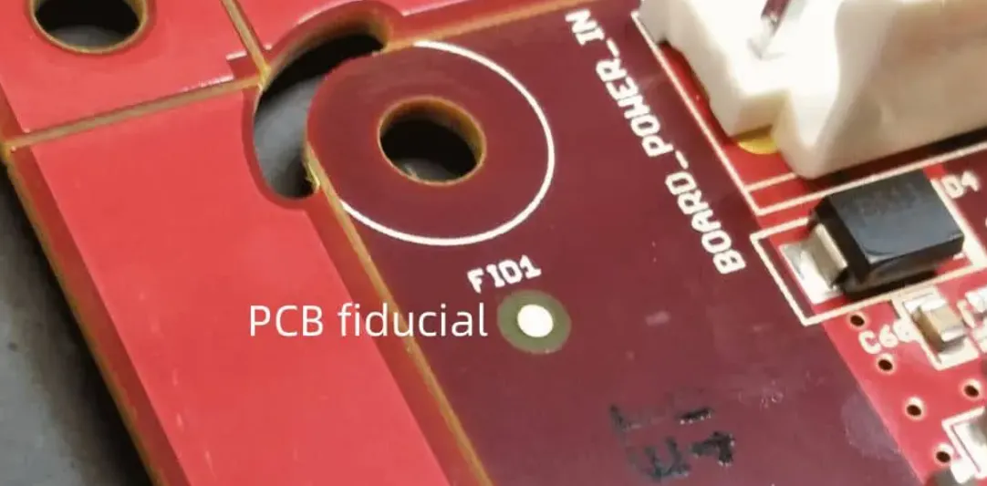
Fiducial marks play a critical role in precise alignment for imaging and placement machines. These targets require clear zones free of components or traces, influencing array spacing. Edge rails, typically added to panels, facilitate conveyor transport and clamping, demanding straight perimeters for stability. Perforations or mouse bites in tabs allow manual or automated breakaway without damaging circuits. Copper balancing on outer layers mitigates plating thickness variations across the panel. These mechanisms ensure PCB manufacturing efficiency by aligning design with fabrication physics.
Depaneling physics further guides shape choices. V-grooves create scored lines for clean snaps along straight paths, ideal for rectangular arrays. Routed slots handle curved outlines but increase cycle times and tool wear. Laser depaneling offers flexibility for intricate shapes yet raises dust concerns near sensitive components. Engineers optimize by selecting shapes that minimize stress risers during separation, preserving trace integrity. Factory experience shows that symmetric panels reduce vibration-induced defects in high-speed lines.
Best Practices for PCB Panel Design
Start with rectangular PCB outlines whenever feasible, as they enable dense packing and simplify tooling paths. Nest boards with minimal gaps, typically matching the smallest feature tolerances, to boost panel yield. Include breakaway tabs on non-critical edges, spaced evenly to distribute forces during depaneling. Position fiducials in corners, at least two per panel, with identical sizes for consistent machine vision. Avoid placing high-density components or fine-pitch parts near panel edges to prevent damage from clamping or routing.
Orient arrays to align golden fingers or connectors outward for easy testing access. Mirror alternate rows to optimize space for odd-length boards, enhancing PCB array optimization. Balance copper pour across the panel to equalize plating currents and reduce thickness gradients. Simulate warpage using finite element analysis early, adjusting stackups if bow exceeds acceptability per IPC-A-600K. Specify depaneling methods in fabrication notes, ensuring compatibility with shape complexity.
For cost-effective PCB manufacturing shapes, prioritize v-scoring over full routing for linear separations, cutting machining time significantly. Use perforated tabs with half-moon cutouts to ease manual separation without burrs. Test panel prototypes for yield before full runs, verifying alignment and stability. Factories recommend square or rectangular panels to match standard fixtures, streamlining workflows. Document rail widths and fiducial offsets clearly to avoid misinterpretation.
Integrate quality checks like electrical testing on panels before depaneling to catch defects early. These practices collectively drive PCB manufacturing efficiency, reducing scrap rates and turnaround times.
Challenges in Complex Shapes and Troubleshooting Solutions
Irregular PCB shapes pose puzzles in panelization due to nesting inefficiencies and depaneling stresses. Curved or polygonal outlines waste space between boards, lowering array density and inflating material costs. Solutions involve approximating shapes with bounding rectangles or using flexible tab configurations. Engineers troubleshoot by iterating layouts in design software, aiming for over 80% panel utilization without fabricating metrics.
Stress from asymmetric shapes during reflow can exceed bow limits, violating performance specs. Redistribute mass via dummy copper fills or symmetric mirroring to counteract. Depaneling irregular panels risks microcracks near tabs if perforations are undersized. Opt for laser or waterjet methods for precision, though routing suffices for prototypes. Factory insights stress previewing Gerber files for overlaps or thin webs that fail under torque.
Component proximity to edges amplifies risks from handling vibrations. Relocate vias and passives inward, maintaining signal paths intact. For multi-up panels with mixed shapes, standardize tab lengths to uniform separation forces. These targeted fixes enhance PCB shape panelization reliability.
Another hurdle is thermal mismatch in mixed-material panels, but single-material arrays avoid this. Monitor plating uniformity via cross-section analysis post-fabrication. Proactive design reviews catch these issues, ensuring cost-effective outcomes.
Conclusion
Optimizing PCB shapes for panelization unlocks substantial gains in manufacturing efficiency and cost control. Rectangular forms and strategic array layouts maximize yields while simplifying depaneling. Best practices like balanced copper, precise fiducials, and method-specific edges align with factory capabilities. Standards such as IPC-6012E and IPC-A-600K provide benchmarks for quality assurance. Electrical engineers benefit from factory-driven approaches that prioritize producibility. Implementing these strategies resolves panelization puzzles, delivering robust boards ready for assembly.
FAQs
Q1: What factors most influence PCB shape panelization success?
A1: Key factors include board outline regularity, array density, and depaneling method compatibility. Rectangular shapes enable tighter packing for better PCB manufacturing efficiency, while fiducials ensure alignment. Factories stress edge clearances to avoid stress during separation. Balanced designs per IPC guidelines minimize warpage, supporting high-volume runs without rework.
Q2: How does PCB panel design impact overall manufacturing costs?
A2: Efficient PCB panel design reduces material waste and processing times through optimized arrays. Dense layouts cut per-board expenses, especially for small quantities. Choosing v-scoring over routing lowers tooling costs for straight shapes. Poor designs increase scrap, inflating totals, so prioritizing space utilization drives cost-effective PCB manufacturing shapes.
Q3: What are common depaneling options for PCB array optimization?
A3: V-scoring works best for linear separations on rectangular panels, offering clean breaks. Tab routing with perforations suits irregular outlines, balancing flexibility and strength. Laser methods provide precision for complex shapes but require dust mitigation. Select based on volume and edge access to enhance PCB manufacturing efficiency.
Q4: Why avoid components near panel edges in PCB shape panelization?
A4: Edges endure clamping, routing, and handling stresses that risk damage to nearby parts. Minimum clearances protect fine-pitch devices and traces from burrs or vibrations. This practice upholds IPC-A-600K acceptability, preventing yield losses. Factory standards mandate offsets for reliable PCB array optimization.
References
IPC-6012E — Qualification and Performance Specification for Rigid Printed Boards. IPC, 2017
IPC-A-600K — Acceptability of Printed Boards. IPC, 2020
IPC-2221B — Generic Standard on Printed Board Design. IPC, 2003


