Introduction
The PCB board outline definition forms the foundation of any printed circuit board design, dictating how the board interacts with its environment from fabrication through final assembly. Engineers must precisely specify the board shape, size, and boundaries to ensure compatibility with enclosures, mechanical fixtures, and automated handling equipment. Poorly defined outlines lead to manufacturing rejects, assembly misalignments, and field failures, underscoring the need for meticulous attention in the design phase. This article explores PCB outline dimensions, specifications, and tolerances, providing electric engineers with structured insights grounded in industry practices. By mastering these essentials, designers can optimize yield rates and reduce iteration cycles in complex projects. Understanding these elements aligns design intent with fabrication capabilities, minimizing costly revisions.
What Is a PCB Board Outline?
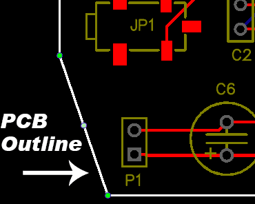
A PCB board outline refers to the external perimeter and internal boundaries that define the physical extent of the printed circuit board. It encompasses the overall shape, such as rectangular, circular, or irregular forms, along with features like cutouts, tabs, and slots. The outline serves as the blueprint for routing, scoring, or beveling processes during manufacturing, directly influencing board handling and edge quality. In design files, the outline layer typically uses a distinct closed contour to communicate these boundaries to fabricators. Electric engineers specify this outline early to accommodate component placement constraints and mechanical integration requirements. Accurate PCB outline definition prevents overlaps with traces or pads, ensuring structural integrity.
Why PCB Outline Specifications Matter
PCB outline specifications directly impact manufacturability, cost, and reliability in high-volume production. Variations in board shape and size affect panel utilization, where inefficient outlines reduce the number of boards per panel and increase scrap. For electric engineers working on dense interconnects, precise boundaries prevent warpage-induced stresses near edges, which can compromise solder joint integrity during reflow. Specifications also guide tooling setup, such as router bit paths or v-groove depths, ensuring clean edges without delamination. In assembly, outline tolerances align boards with pick-and-place fiducials and stencils, reducing placement errors. Ultimately, robust specifications bridge design and fabrication, aligning with performance classes defined in standards like IPC-6012E.
Improperly defined outlines lead to challenges in thermal management, as irregular shapes alter heat dissipation patterns across the board. Engineers must consider how outline features influence airflow in enclosures or conformal coating coverage. Specifications also dictate material utilization, where overly complex boundaries escalate tooling costs without proportional benefits. By prioritizing standard shapes when possible, teams streamline quoting and lead times. This forward-thinking approach enhances supply chain predictability for time-sensitive projects.
Key Elements of PCB Outline Dimensions
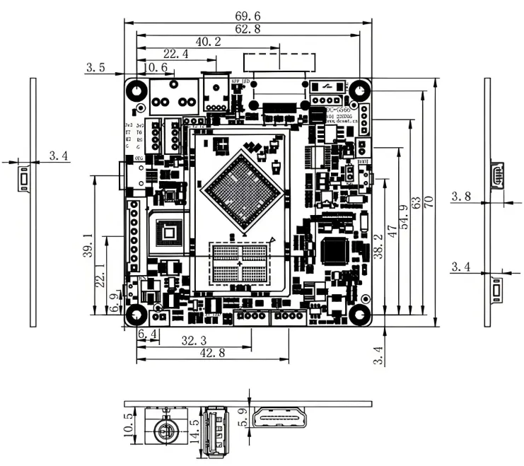
PCB outline dimensions include length, width, thickness, and any protrusions or recesses that form the board's footprint. Rectangular outlines dominate due to their simplicity in nesting and handling, but custom dimensions suit applications like wearables or avionics. Engineers specify overall dimensions from edge to edge, accounting for panelization where multiple boards share borders. Internal cutouts for connectors or heat sinks require coordinated dimensioning to maintain rigidity. Dimensions must balance electrical performance with mechanical stability, avoiding thin sections prone to flexing.
When defining dimensions, consider the board's aspect ratio, which influences milling stability and edge straightness. Tall, narrow boards demand reinforced tabs or breakaway rails to prevent distortion during depanelization. Outline dimensions also integrate with stack-up requirements, ensuring vias and planes align without encroaching on boundaries. Electric engineers use these specs to simulate fit within housings, preempting tolerance stack-up issues. Clear dimension callouts in fabrication drawings eliminate ambiguity, fostering consistent output across vendors.
PCB Outline Tolerances: Critical Considerations
PCB outline tolerances represent the allowable deviation from nominal dimensions, categorized by edge type and fabrication method. Routing offers tighter control than scoring, with tolerances varying by board class and material thickness. Engineers specify these to accommodate tooling inaccuracies and material expansion during lamination. IPC-A-600H outlines acceptability criteria for edge straightness and corner radii, guiding inspection post-fabrication. Tolerances tighten for high-reliability boards, where micron-level precision supports fine-pitch components.
Factors like panel size and quantity influence achievable tolerances, as larger arrays amplify cumulative errors. Electric engineers mitigate this by incorporating fiducials outside the outline for alignment reference. Tolerances also apply to internal features, ensuring slots mate reliably with mating hardware. Overly aggressive specs increase costs, so baseline values suffice for most prototypes. Balancing tolerances with yield optimizes project economics without sacrificing function.
Common Board Shapes and Boundary Features
Rectangular boards provide baseline efficiency, with straight edges ideal for automated handling and testing. Irregular outlines accommodate ergonomic curves or mounting holes in compact devices, though they complicate tooling paths. Boundaries include chamfers to reduce stress concentrations at corners, preventing cracks in flex-prone applications. Tabs and castellations enable panel sharing, where scored lines define breakaway points. Engineers select shapes based on downstream processes, favoring routable features for clean separation.
Circular or polygonal outlines suit RF antennas or optical modules, demanding radial symmetry for performance. Internal boundaries like moats isolate sections electrically while maintaining mechanical unity. Vias near edges require offset distances to avoid stub exposure during trimming. Complex boundaries benefit from stepped routing to minimize burrs. These choices reflect trade-offs in design freedom versus fabrication feasibility.
Best Practices for Specifying PCB Outlines
Start with a dedicated outline layer in your design software, using 0-width lines for unambiguous contours. Define dimensions in the fabricator's preferred units, typically millimeters or mils, with bidirectional tolerances. Incorporate breakaway tabs at least 2 mm wide for stability, positioned away from critical components. Specify edge finish, such as routed with specific bit diameter, to control radius consistency. For multilayer boards, verify outline alignment across cores to prevent layer shift.
Communicate specifications via comprehensive drawings, including cross-sections for thickness uniformity. Simulate panelization early to maximize yield, using symmetric arrays for uniform stress. Electric engineers should reference IPC-2221B for design guidelines on boundary clearances. Prototype irregular outlines to validate tolerances before scaling. Iterate feedback from trial runs refines specs for production.
Troubleshooting Outline-Related Issues
Misaligned outlines often stem from artwork scaling errors or mismatched gerber scaling factors. Inspect incoming panels for warpage, which distorts boundaries beyond tolerance. Burrs from dull tooling create handling hazards, resolvable by post-rout deburring specs. Thin webs between cutouts fracture easily, so widen them per rigidity needs. Engineers diagnose via CMM measurements, correlating deviations to process parameters.
Assembly rejects trace to outline oversize, jamming fixtures; counteract with conservative tolerances. Thermal expansion mismatches exacerbate boundary gaps in hybrid modules. Document root causes in ECNs to prevent recurrence. Collaborative reviews with fabricators preempt these pitfalls.
Conclusion
Mastering PCB board outline definition, dimensions, specifications, and tolerances empowers electric engineers to deliver robust, manufacturable designs. From simple rectangles to intricate contours, precise boundaries ensure seamless progression through fabrication, assembly, and deployment. Adhering to standards like IPC-6012E and IPC-A-600H minimizes risks while optimizing costs. Proactive specification and validation practices yield higher first-pass success rates. As projects grow in complexity, these essentials remain pivotal for innovation and reliability.
FAQs
Q1: What factors influence PCB outline tolerances?
A1: PCB outline tolerances depend on fabrication method, board class, material thickness, and panel size. Routing achieves finer control than v-scoring, with standards like IPC-A-600H defining acceptability for edge quality. Electric engineers specify tighter tolerances for high-density interconnects to support precise assembly. Balancing these ensures manufacturability without excessive cost. Always align specs with performance requirements.
Q2: How do you define PCB outline dimensions in design files?
A2: Define PCB outline dimensions using a closed contour on a dedicated layer in CAD software, labeling length, width, and features clearly. Include bidirectional tolerances and units for clarity. Account for panelization tabs to aid depanelization. Verify against enclosure fit via 3D models. This PCB board outline definition prevents scaling errors in gerber output.
Q3: Why are PCB outline specifications crucial for assembly?
A3: PCB outline specifications ensure boards align with stencils, fixtures, and pick-and-place machines, minimizing placement offsets. Irregular shapes require fiducials near boundaries for reference. Tolerances accommodate minor variations from lamination. Poor specs lead to solder defects or handling damage. Engineers prioritize these for high-yield SMT processes.
Q4: What are common PCB outline shapes and their uses?
A4: Common shapes include rectangular for standard applications, circular for RF modules, and irregular for custom enclosures. Tabs facilitate panelization, while chamfers reduce stress. Select based on mechanical and electrical needs. PCB outline dimensions must support downstream trimming without component damage. Simplicity aids cost control.
References
IPC-6012E — Qualification and Performance Specification for Rigid Printed Boards. IPC, 2015
IPC-A-600H — Acceptability of Printed Boards. IPC, 2014
IPC-2221B — Generic Standard on Printed Board Design. IPC, 2012


