Introduction
Power integrity analysis for space PCBs stands as a critical step in designing electronics that must withstand the unforgiving conditions of space missions. Spacecraft electronics face extreme thermal cycling, radiation exposure, mechanical vibrations, and vacuum environments, all of which amplify the risks associated with power delivery instability. Unstable power can lead to voltage fluctuations that cause logic errors, component failures, or complete system shutdowns, potentially jeopardizing multimillion-dollar missions. Effective power distribution network (PDN) design ensures that every integrated circuit receives clean, stable voltage under all operating scenarios. This article explores the principles, challenges, and best practices for power integrity in spacecraft PCBs, tailored for electrical engineers seeking reliable performance. By prioritizing PDN design for space electronics from the outset, designers can mitigate risks and enhance mission longevity.
What Is Power Integrity Analysis and Why It Matters for Spacecraft Electronics
Power integrity analysis evaluates the ability of a PCB's PDN to deliver stable voltage to active components while minimizing noise, ripple, and drops. In spacecraft applications, where power budgets are tightly constrained and redundancy is often limited, even minor PDN imperfections can cascade into system-wide failures. Radiation-induced single-event effects exacerbate power noise sensitivity, making voltage drop analysis and ground bounce mitigation essential. Engineers must consider the PDN as an interconnected system of planes, traces, vias, and capacitors that collectively form the power backbone. Poor power integrity manifests as excessive impedance peaks, leading to electromagnetic interference that couples into signal lines. For space PCBs, adherence to rigorous qualification processes underscores the need for proactive analysis to ensure operational reliability over years or decades.
The stakes in space electronics demand that power integrity analysis for space PCBs integrates with overall signal integrity efforts early in the design cycle. Missions operate without repair options, so PDN weaknesses undetected pre-launch become mission-ending defects. Thermal expansion mismatches between materials can alter PDN geometry, introducing variable resistance and inductance. Vibration during launch stresses solder joints and vias in the PDN, potentially creating intermittent power paths. Ground bounce, arising from simultaneous switching of multiple outputs, distorts reference potentials across the board. Thus, robust PDN design for space electronics directly correlates with mission success rates.
Technical Principles of Power Integrity in Spacecraft PCBs
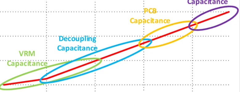
At its core, power integrity hinges on maintaining low PDN impedance across a wide frequency spectrum, from DC to gigahertz ranges relevant to modern spacecraft processors. DC voltage drop analysis reveals resistive losses in traces and planes under maximum load currents, where even milliohms matter due to space's low-power margins. Inductive effects dominate at higher frequencies, causing voltage overshoot or undershoot during transients. In spacecraft PCBs, material selection for low outgassing and radiation tolerance influences dielectric properties, affecting capacitance and loss tangents in the PDN. Resonance between plane pairs and decoupling capacitors can amplify noise if not tuned properly. Understanding these mechanisms allows engineers to predict and verify PDN behavior through targeted simulations.
Ground bounce mitigation addresses simultaneous switching noise (SSN), where multiple drivers toggle states, drawing sharp current pulses through package and board inductances. This creates a shifting ground potential that appears as noise on all I/O signals referenced to it, degrading margins in high-speed interfaces common in spacecraft telemetry. The phenomenon worsens in multi-layer stacks with split planes or long return paths. Decoupling capacitor placement plays a pivotal role by providing localized charge reservoirs to supply transient currents, bypassing board-level inductances. Effective placement minimizes loop inductance, typically achieved with vias directly under capacitor pads. In space environments, capacitor reliability under thermal extremes and radiation further complicates selection.
Voltage drop analysis extends to dynamic AC scenarios, where ripple from switching regulators propagates through the PDN. Plane splitting for multiple rails introduces slot resonances, coupling noise between domains. Spacecraft power systems often use point-of-load converters, amplifying the need for low-impedance paths to prevent droop during load steps. Thermal management intersects here, as elevated temperatures increase conductor resistivity by up to 50% per 100°C rise. Engineers model these using equivalent circuit approximations or field solvers to quantify drops. Consistent low impedance below target profiles ensures components operate within datasheet tolerances.
Practical Solutions and Best Practices for PDN Design in Space Electronics
Start PDN design for space electronics with dedicated power and ground planes on inner layers, maximizing capacitance through tight plane spacing under 10 mils where feasible. Wide traces and multiple vias in parallel reduce DC resistance, targeting voltage drops below 5% of supply rails. Avoid splits in planes near high-current paths to prevent current crowding and hotspots. For multi-rail systems, use stitching vias along split boundaries to equalize potentials and suppress resonances. IPC-2221 guidelines on conductor sizing and spacing provide a foundation for these layouts, ensuring mechanical robustness alongside electrical performance.
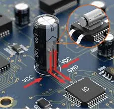
Decoupling capacitor placement demands proximity to IC power pins, ideally within 1-2 mm, using arrays of values from 0.01 μF to 10 μF to cover frequency bands. Employ low-ESL ceramic types with via-in-pad connections for minimal inductance loops under 1 nH. In spacecraft PCBs, select capacitors rated for extended temperature ranges and low radiation degradation. Distribute them evenly across the die shadow to handle spatially varying current demands. Bulk capacitors near voltage regulators handle low-frequency stability. Verification through time-domain reflectometry confirms effective bypassing.
Ground bounce mitigation benefits from solid ground planes providing low-inductance returns, minimizing simultaneous switching effects. Series damping resistors on outputs or controlled slew rates at drivers reduce di/dt, softening current edges. Power island isolation with guard traces prevents noise spillover. For voltage drop analysis, iterate stackups to balance plane usage with routing needs, prioritizing high-current nets on thick copper layers. J-STD-001 requirements for soldering ensure reliable capacitor and via joints under vibration. Post-layout extraction feeds into PI tools for impedance and droop checks against space-qualified margins.
Advanced techniques include embedded capacitors in the stackup for ultra-low inductance, though manufacturing yields demand caution. Hybrid PDNs with both local and global decoupling optimize cost and space. Thermal vias under hot spots dissipate heat without compromising PDN integrity. Qualification per IPC-6012 performance specs validates these designs through accelerated life testing. Regular design reviews catch PDN pitfalls early.
Troubleshooting Common PDN Issues in Spacecraft Electronics
Engineers often encounter excessive ripple traced to inadequate bulk decoupling or regulator instability. Measure PDN impedance profiles to identify peaks, then add targeted capacitors to fill valleys. Ground bounce symptoms like bit errors in data buses point to return path inductance; consolidate grounds and add stitching. Voltage drops exceeding budgets during hot-soak tests signal undersized planes, remedied by thickening copper or paralleling paths. Radiation testing reveals soft errors worsened by PI noise, necessitating margin stacking. Systematic logging of current profiles from simulations guides fixes.
A typical case involves a processor board failing thermal-vacuum quals due to 100 mV droop under load. Analysis showed via bottlenecks in the PDN; adding redundant vias and reshaping planes resolved it. Decoupling audits ensure coverage, while S-parameter models predict interactions. Collaborative reviews with manufacturing align designs to process capabilities. These steps turn potential failures into robust solutions.
Conclusion
Power integrity analysis for space PCBs demands a holistic approach to PDN design for space electronics, integrating voltage drop analysis, ground bounce mitigation, and precise decoupling capacitor placement. By leveraging solid planes, strategic components, and standards-compliant practices, engineers achieve stable power delivery critical for mission success. Early analysis prevents costly respins, while best practices ensure resilience against space hazards. Prioritizing these elements elevates spacecraft electronics reliability, safeguarding data and operations in orbit.
FAQs
Q1: What role does decoupling capacitor placement play in power integrity analysis for space PCBs?
A1: Decoupling capacitor placement minimizes loop inductance, supplying transient currents locally to ICs and stabilizing the PDN. In space electronics, place them within millimeters of power pins using low-ESL types and via-in-pad for optimal performance. This reduces voltage ripple and ground bounce, essential under radiation and thermal stress. Arrays spanning decades cover broad frequencies, verified through impedance profiling. Proper implementation per design guidelines enhances overall reliability.
Q2: How does voltage drop analysis impact PDN design for space electronics?
A2: Voltage drop analysis quantifies IR losses in traces and planes under peak loads, ensuring components stay within voltage tolerances. Spacecraft PDNs target drops below 5% using wide conductors and multi-via stitching. DC modeling accounts for temperature rises, preventing logic upsets. Integration with thermal analysis refines stackups. This proactive step aligns with qualification standards for long-term stability.
Q3: What are effective strategies for ground bounce mitigation in spacecraft PCBs?
A3: Ground bounce mitigation relies on solid ground planes and close-proximity decoupling to provide low-inductance returns. Limit slew rates and use damping resistors on drivers to curb di/dt. Stitching vias bridge splits, equalizing potentials. PDN impedance below targets suppresses SSN coupling. These practices maintain signal margins in high-speed spacecraft interfaces.
Q4: Why is early PDN design critical for power integrity analysis for space PCBs?
A4: Early PDN design prevents impedance violations that ripple through layout and routing phases. Space constraints amplify the need for plane dedication and capacitor planning upfront. Simulations guide iterations, avoiding respins. Alignment with manufacturing capabilities ensures producibility. This foundation supports robust power delivery across mission lifecycles.
References
IPC-2221B — Generic Standard on Printed Board Design. IPC, 2012
IPC-6012E — Qualification and Performance Specification for Rigid Printed Boards. IPC, 2017
J-STD-001H — Requirements for Soldered Electrical and Electronic Assemblies. IPC, 2018


