Introduction
Precision planting represents a transformative approach in modern agriculture, where data from field sensors guides seeding decisions to optimize crop yields and resource use. Agricultural sensor PCBs form the backbone of these systems, integrating multiple sensors into compact, reliable platforms that withstand harsh outdoor conditions. These boards collect critical data on soil properties, enabling farmers to adjust planting rates and inputs in real time. By focusing on agricultural PCB design for precision planting, engineers can create solutions that reduce waste and boost productivity. This article explores the technical aspects of these PCBs, from component selection to layout strategies, tailored for electric engineers designing robust systems. Understanding these elements ensures systems deliver accurate, actionable insights for variable rate seeding and beyond.
The Role of Agricultural Sensor PCBs in Precision Agriculture
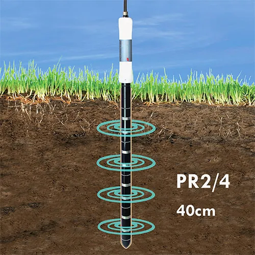
Agricultural sensor PCBs process data from embedded sensors to inform precision planting strategies, directly impacting crop establishment and yield potential. These boards must handle diverse environmental stresses, including moisture, temperature fluctuations, and mechanical vibrations from farm equipment. In precision agriculture, they enable variable rate seeding by mapping soil variability across fields, allowing planters to deposit optimal seed densities. Engineers prioritize low-power operation to support battery or solar-powered deployments in remote areas. Reliability under field conditions separates effective designs from failures, as poor performance leads to data gaps and misguided decisions. Adhering to standards like IPC-6012E for qualification and performance of rigid printed boards ensures these PCBs meet demanding requirements.
Soil monitoring PCBs track parameters such as moisture, pH, and nutrient levels, feeding data into central systems for analysis. Integration with wireless modules allows real-time transmission to farm management software. This connectivity supports automated adjustments during planting operations. Designers must balance size constraints with signal integrity to avoid noise in sensor readings. Field-deployed boards often incorporate protective coatings to prevent corrosion from soil acids or fertilizers. Overall, these PCBs bridge the gap between raw environmental data and farm-level actions.
Key Sensors and PCB Component Selection for Soil Monitoring
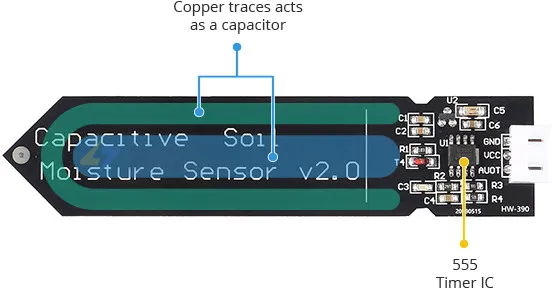
Selecting components for soil monitoring PCBs requires careful consideration of accuracy, durability, and power efficiency in contaminated, wet environments. Capacitive soil moisture sensors, using PCB traces as electrodes, offer non-corrosive alternatives to resistive types, minimizing degradation over time. pH sensors typically employ ion-selective electrodes interfaced via analog front-ends with low-noise amplifiers to handle weak signals. Nutrient sensors for nitrogen, phosphorus, and potassium detection often rely on electrochemical cells or optical methods, demanding stable voltage references and precise analog-to-digital converters. Microcontrollers with integrated ADCs, such as low-power ARM-based units, centralize data processing while supporting multiple sensor inputs.
Power management components play a crucial role, with low-dropout regulators and efficient DC-DC converters ensuring stable supply amid varying battery voltages. Wireless transceivers operating in sub-GHz bands provide long-range communication with minimal power draw, essential for widespread field networks. Passive components like high-precision resistors and capacitors must tolerate humidity, often specified for extended temperature ranges. Engineers troubleshoot component failures by verifying thermal dissipation and ESD protection, using diodes or TVS devices at interfaces. Conformal coatings post-assembly enhance longevity, but component selection upfront prevents issues like delamination from moisture ingress. This methodical approach aligns with JEDEC J-STD-020E for handling moisture-sensitive devices during assembly.
Temperature and conductivity sensors complement core soil metrics, using thermistors or RTDs calibrated for buried operation. Engineers select SMD packages for compactness, ensuring reflow compatibility. Signal conditioning circuits filter noise from electromagnetic interference near tractors or irrigation pumps. Firmware optimizes sampling rates to conserve energy without sacrificing resolution. Testing involves simulated soil immersion to validate long-term stability.
Sensor PCB Layout Guidelines for Optimal Performance
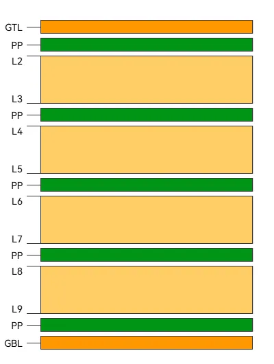
Sensor PCB layout guidelines emphasize signal integrity, thermal management, and manufacturability to support reliable precision planting data. Place analog sensors close to their conditioning circuits to minimize trace lengths and reduce noise pickup. Dedicated ground planes separate analog and digital sections, preventing return path interference. Power traces should follow wide, short paths with decoupling capacitors near every IC pin for stability. In multi-layer boards, route high-speed digital signals on inner layers, shielding sensitive analog lines on the top layer.
For wireless integration, position antennas away from noisy power sections, adhering to 50-ohm impedance matching. Vias under sensors require careful placement to avoid shorts in conformal-coated assemblies. Thermal vias dissipate heat from power regulators, preventing hotspots in enclosed probes. Engineers follow controlled impedance for data lines to maintain accuracy in real-time nutrient analysis PCBs. Solder mask openings over sensor electrodes ensure proper exposure without bridging. These practices mitigate common issues like crosstalk or ground bounce during field vibrations.
Routing density increases with added sensors, so use autorouters judiciously, followed by manual reviews for DRC violations. Fiducials aid pick-and-place accuracy in assembly. Edge connectors or headers facilitate integration into probes, with strain relief for cabling. Post-layout simulations verify EMI compliance. Layout revisions often stem from prototype testing, where flexing reveals trace cracks.
Enabling Real-Time Nutrient Analysis and Variable Rate Seeding
Real-time nutrient analysis PCBs process electrochemical or spectroscopic data to quantify soil macronutrients, enabling immediate adjustments in fertilizer application. These boards feature multi-channel potentiostats for simultaneous ion measurements, with firmware applying calibration curves for accuracy. Data fusion algorithms combine nutrient profiles with moisture and pH readings, generating maps for variable rate seeding systems. Integration with GPS modules timestamps data for zonal prescriptions, where seeders adjust rates based on fertility zones.
PCBs for variable rate seeding incorporate actuators or CAN interfaces to control planter motors directly. Low-latency processing ensures synchronization with tractor speed. Battery management extends uptime during long planting sessions. Troubleshooting involves logging errors for root cause analysis, such as sensor drift from biofouling. Engineers design modular layouts for easy sensor upgrades. ISO 9001:2015 quality management principles guide consistent production for field scalability.
High-resolution ADCs capture subtle nutrient gradients, critical for hybrid vigor optimization. Edge computing reduces cloud dependency, processing data onboard. Security features like encrypted transmissions protect against tampering. Field calibration routines maintain precision over seasons.
Best Practices and Troubleshooting for Agricultural PCBs
Agricultural PCB design for precision planting demands robust materials like high-Tg FR-4 laminates to withstand thermal cycling from day-night shifts. Conformal coatings, such as acrylic or silicone, provide IP67-level protection against dust and water. Assembly follows IPC-A-600K acceptability criteria for visual and dimensional quality. Potting compounds encase boards in probes, enhancing shock resistance. Engineers perform accelerated life testing simulating years of exposure.
Common troubleshooting includes intermittent connectivity from oxidation, resolved by gold plating contacts. Power budgeting prevents brownouts during transmission bursts. Firmware updates via OTA mitigate software bugs. Supply chain selection ensures RoHS compliance for sustainability. Documentation of design files supports iterative improvements.
Conclusion
Agricultural sensor PCBs drive precision planting by delivering reliable data for optimized seeding and resource use. From component selection for soil monitoring to sensor PCB layout guidelines, thoughtful design maximizes system performance in challenging environments. Real-time nutrient analysis PCBs and those for variable rate seeding exemplify how engineering precision translates to higher yields. Adhering to industry standards ensures longevity and trust. Electric engineers can leverage these principles to innovate further, supporting sustainable farming practices.
FAQs
Q: What are key sensor PCB layout guidelines for agricultural applications?
A: Sensor PCB layout guidelines prioritize analog-digital separation with dedicated ground planes to minimize noise in soil data. Place sensors near amplifiers for short traces, and use thermal vias under power components. Impedance control on wireless paths supports reliable transmission. Conformal coatings protect against moisture, aligning with harsh field needs. These steps enhance accuracy in precision planting systems.
Q: How does PCB component selection impact soil monitoring effectiveness?
A: PCB component selection for soil monitoring favors capacitive sensors and low-power MCUs for durability and efficiency. Electrochemical cells with stable references detect nutrients accurately. ESD protection and humidity-tolerant passives prevent failures. Balanced power management extends battery life in remote deployments. This selection ensures consistent performance for variable rate seeding decisions.
Q: What role do real-time nutrient analysis PCBs play in precision agriculture?
A: Real-time nutrient analysis PCBs enable on-the-spot NPK and pH measurements via multi-channel interfaces. Data processing supports immediate fertilizer adjustments during operations. Wireless integration feeds into farm analytics for zoning. Robust designs with coatings handle soil exposure. They optimize inputs, reducing costs and environmental impact in precision planting.
Q: Why is agricultural PCB design critical for variable rate seeding?
A: Agricultural PCB design for precision planting integrates sensors with control interfaces for dynamic seed rate changes based on soil data. Compact layouts fit planter modules while maintaining signal integrity. Low-latency processing syncs with machinery. Ruggedization ensures vibration resistance. This design maximizes yield uniformity across variable fields.
References
IPC-6012E — Qualification and Performance Specification for Rigid Printed Boards. IPC, 2017
JEDEC J-STD-020E — Moisture/Reflow Sensitivity Classification. JEDEC, 2014
IPC-A-600K — Acceptability of Printed Boards. IPC, 2020
ISO 9001:2015 — Quality Management Systems. ISO, 2015


