Introduction
Power distribution forms the backbone of any printed circuit board, ensuring components receive stable voltage under varying loads. In PCBs, the power distribution network (PDN) manages current flow from entry points to loads, directly impacting overall performance. Different PCB form factors, from standard rectangular boards to flexible or irregular shapes, present unique challenges for maintaining power integrity. Engineers must optimize PCB power planes and routing to minimize voltage drop, especially in high-current designs where resistance and inductance can degrade signals. Poor PDN design leads to issues like excessive heating, signal noise, and component failure, making optimization critical for reliable operation. This article explores strategies for effective power distribution across diverse form factors, drawing on established engineering principles.
Understanding Power Distribution Networks in PCBs
A power distribution network in a PCB encompasses power planes, traces, vias, and decoupling capacitors that deliver DC power while suppressing noise. PCB power planes, typically solid copper layers dedicated to voltage rails, offer low resistance paths compared to thin traces. The PDN must handle both steady-state DC currents and transient AC demands from switching components. Voltage drop, or IR drop, occurs due to resistive losses along these paths, potentially causing undervoltage at loads. Power integrity PCB design focuses on keeping impedance low across frequencies to prevent ripple and ground bounce. In high-current PCB design, these elements become even more vital to avoid hotspots and ensure thermal stability.
Form factors influence PDN effectiveness because board geometry affects current path lengths and plane continuity. Rectangular boards allow straightforward plane pours, while elongated or curved shapes demand careful partitioning to avoid splits. Engineers evaluate PDN performance through metrics like target impedance and maximum allowable voltage drop, typically under 5% for most digital rails. Adhering to guidelines in IPC-2221 helps standardize these aspects for consistent results.
Technical Principles of Power Distribution
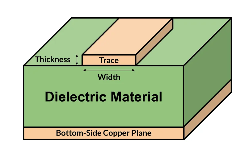
At DC, power distribution relies on minimizing resistance in PCB power planes and traces. Resistance follows Ohm's law, where voltage drop equals current times resistance, so wider conductors and thicker copper reduce losses. For instance, in multi-layer boards, internal planes provide shorter return paths, lowering inductance. External traces suit low-current signals but falter in high-current scenarios due to higher resistance per unit length. Cross-sectional area, determined by copper weight and width, directly scales current capacity.
AC behavior introduces impedance from plane inductance and capacitance between layers. Plane pairs act as distributed capacitors, stabilizing voltage during transients. In non-ideal geometries, voids or splits in planes create high-impedance zones, amplifying noise. Simulations reveal these effects, but analytical models estimate inductance as roughly length over width times a factor. For power integrity PCB analysis, engineers target impedance profiles below 0.1 ohms up to GHz frequencies.
Different form factors alter these principles. Long, thin boards experience greater longitudinal drops, necessitating segmented planes or parallel paths. Circular or conformal PCBs, common in wearables, require radial power distribution to equalize paths from center to edges.
Power Distribution Challenges in Various PCB Form Factors
Standard rectangular PCBs simplify PDN design with uniform plane fills and orthogonal routing. Power enters via edge connectors, spreading evenly across full layers. However, high aspect ratios in rectangular boards, like those in servers, amplify drops along the length. Engineers counter this by adding intermediate power pins or vias arrays.
Elongated or strip-like form factors, used in LED strips or sensors, face pronounced end-to-end voltage gradients. Current crowds toward loads, starving distant components. Flexible PCBs introduce dynamic bending, which stresses traces and alters resistance over flex cycles. Rigid-flex hybrids combine rigid sections for heavy components with flex tails, requiring transitioned PDN layouts to maintain continuity.
Irregular shapes, such as those in automotive modules or medical devices, complicate plane pours due to cutouts and contours. Voids around mounting holes disrupt current flow, creating bottlenecks. High-density interconnect (HDI) boards with fine-pitch vias demand microvias for PDN stitching, balancing density with low impedance.
Best Practices for Optimizing PCB Power Planes
Start with dedicated power and ground plane pairs on adjacent layers for tight coupling and low inductance. Fill planes solidly rather than hatching to minimize resistance, reserving hatches for thermal relief in high-power zones. Stitch planes with via arrays every 1/20th wavelength at highest frequencies to equalize potentials and reduce slot radiation.
For minimizing voltage drop in PCB designs, employ multiple voltage entry points and wide spokes from connectors to planes. Use heavier copper weights, like 2 oz/ft2 or more, in high-current PCB design layers. Decoupling capacitors placed near loads form local reservoirs, handling transients without drawing from distant planes.
In different form factors, adapt pours to contours while avoiding splits under signals. For elongated boards, add longitudinal ribs or parallel planes. IPC-2152 provides charts for trace and plane current capacities based on temperature rise, guiding copper selection without overdesign.
Strategies for Power Integrity and High-Current Design
Power integrity PCB verification involves checking DC drops under max load and AC impedance profiles. Keep plane resistance below milliohms by maximizing fill and minimizing vias in current paths. For high-current paths, calculate capacities per IPC-2152, accounting for external versus internal heating differences.
In flexible form factors, reinforce PDN with wider traces and adhesive layers to prevent fatigue. Use blind or buried vias in rigid-flex to shorten paths. Simulate PDN early, iterating on via density and cap placement for target impedance.
Troubleshoot common issues like excessive drop by measuring plane DC resistance with Kelvin probes. Ground bounce signals poor return paths; fix with denser stitching.
Conclusion
Optimizing power distribution across PCB form factors demands a holistic PDN approach, from plane sizing to via placement. PCB power planes enable low-impedance delivery, while careful routing minimizes voltage drop PCB issues. High-current PCB design benefits from standards like IPC-2152 for safe capacities. Power integrity PCB practices ensure stability in diverse geometries, from rigid rectangles to flex circuits. Engineers achieve reliable boards by balancing form factor constraints with these principles, enhancing performance and longevity.
FAQs
Q1: How do PCB power planes improve power distribution network PCB performance?
A1: PCB power planes provide low-resistance, wide-area conductors that distribute current evenly, reducing IR drop compared to traces. They form parallel-plate capacitors with ground planes, stabilizing voltage during transients. In multi-layer boards, internal planes lower inductance for better high-frequency response. This setup maintains power integrity across loads, essential for dense designs.
Q2: What techniques minimize voltage drop PCB in elongated form factors?
A2: Use multiple power entry points and segmented planes with stitching vias to shorten paths. Thicker copper and parallel routing balance loads along the length. Decoupling caps at intervals prevent cumulative drops. Simulate DC analysis to verify under max current. These steps ensure uniform voltage in strip-like boards.
Q3: Why is power integrity PCB critical in high-current PCB design?
A3: Power integrity prevents noise, ripple, and undervoltage that cause failures in high-current scenarios. Low PDN impedance handles transients without excessive drop. Proper plane pairing reduces EMI and ground bounce. Adhering to capacity limits avoids overheating. This safeguards component reliability in demanding applications.
Q4: How does form factor affect high-current PCB design PDN?
A4: Irregular shapes require contour-following planes to avoid splits and bottlenecks. Flexible forms need reinforced conductors for bend cycles. Rectangular boards allow full pours, but elongated ones demand ribs. Vias and copper weight adapt to geometry for even distribution. This maintains integrity despite shape variations.
References
IPC-2221B — Generic Standard on Printed Board Design. IPC, 2003
IPC-2152 — Standard for Determining Current Carrying Capacity in Printed Board Design. IPC, 2009


