Introduction
Router PCB assembly and switch PCB manufacturing process demand precision due to the high-density interconnects and complex components in networking equipment. These boards handle massive data throughput, requiring multilayer stacks with fine-pitch ball grid arrays (BGAs) and surface-mount technology (SMT) components. Assembly challenges such as warpage, solder defects, and thermal mismatches can lead to yield losses and field failures. Engineers face SMT challenges including accurate paste deposition and component placement under tight tolerances. Reflow soldering optimization becomes critical to ensure reliable joints without compromising signal integrity. This article explores these hurdles and provides practical strategies to enhance router PCB assembly success.
Why Router and Switch PCBs Present Unique Assembly Demands
Router and switch PCBs operate in demanding environments with high-speed signals up to 400 Gbps, necessitating controlled impedance and minimal crosstalk. They typically feature 20 or more layers, HDI vias, and large BGAs with over 2000 pins at pitches below 0.8 mm. The switch PCB manufacturing process involves integrating processors, PHY chips, and memory in dense arrays, amplifying risks during SMT processes. Reliability is paramount, as failures disrupt network operations in data centers or enterprises. Assembly must align with class 3 requirements for high-performance electronics. Addressing these demands early in design prevents costly rework.
Core Technical Challenges in Router PCB Assembly
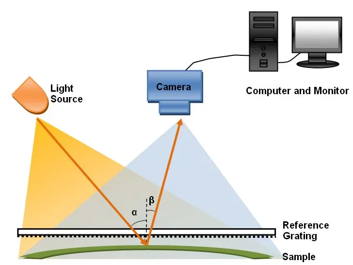
One primary issue in router PCB assembly is PCB warpage from asymmetric copper distribution and CTE mismatches between materials. During reflow, this warpage causes BGA misalignment, leading to open joints or bridges. High component density exacerbates placement errors, where pick-and-place machines struggle with 01005 passives or 0.4 mm pitch QFNs. Solder paste printing inconsistencies, such as insufficient volume or smearing, compound these problems. Thermal gradients in thick boards further distort reflow profiles, risking head-in-pillow defects. Engineers must quantify warpage using shadow moire techniques to predict assembly risks.
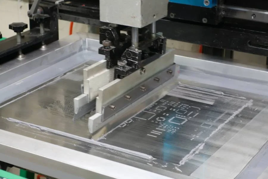
SMT challenges intensify with mixed component heights and large panels, where gravity affects paste flow. Fine-pitch leads demand stencils with apertures reduced by 10-15% for optimal volume. In switch PCB manufacturing process, via-in-pad designs complicate paste release, potentially trapping air voids. Humidity control prevents oxidation, yet moisture absorption in laminates alters dimensions. These factors demand rigorous process controls to maintain first-pass yields above 95%.
Navigating BGA Assembly Complexities
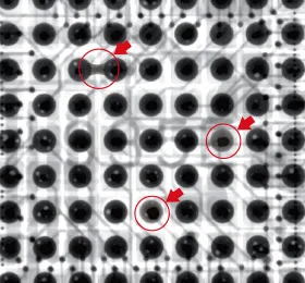
BGA assembly in routers and switches involves high-I/O packages like 45x45 mm grid arrays, where solder ball collapse must stay within 75 microns. Misalignment beyond 25% of pitch voids joints, detectable only via X-ray. IPC-7095 guidelines specify land pattern tolerances and via configurations to minimize defects. Head-in-pillow occurs when balls do not fully wet due to oxide layers or profile spikes. Warpage exceeding 0.75% induces stress cracks post-assembly. Pre-bake and nitrogen reflow mitigate these, but require validation through cross-section analysis.
Bridging risks rise with non-collapsing balls in fine-pitch arrays, demanding Type 5 paste for better release. Inspection challenges persist, as automated optical systems miss subsurface voids. Process windows narrow for lead-free alloys, with peak temperatures controlled to 260°C. Rework demands specialized tools to avoid damaging adjacent components. Consistent BGA assembly hinges on design-for-assembly rules from the outset.
Tackling SMT Challenges in High-Density Switch PCBs
SMT challenges in switch PCB manufacturing process include tombstoning of small passives from rapid preheat ramps exceeding 3°C/s. Insufficient paste height leads to cold joints, while excess causes shorts in 0.5 mm pitch areas. Stencil misalignment by 50 microns disrupts volume control, especially on stepped stencils for BGAs and QFPs. Component shifting during transit to reflow ovens affects yields. Fiducials must exceed 1 mm for machine vision accuracy.
Electrostatic discharge threatens sensitive ICs, necessitating grounded handling. Board thickness variations from fabrication tolerances impact placement force. These issues cascade into reflow, amplifying defects. Proactive DFM reviews catch 80% of problems pre-production.
Optimizing Reflow Soldering for Reliable Joints
Reflow soldering optimization starts with profiling to match JEDEC J-STD-020E classifications for moisture sensitivity levels. Preheat soaks flux activators at 150-180°C for 60-120 seconds, preventing thermal shock. Reflow peak holds at 240-260°C for 40-90 seconds above liquidus, ensuring full melt without intermetallic excess. Cooling rates below 6°C/s control grain structure for fatigue resistance. Nitrogen atmospheres reduce dross and oxidation, expanding process windows by 20%.
Oven zoning compensates for board size, with edge cooling fans for uniformity. Validation uses thermocouples at critical locations like corners and BGAs. Profile deviations beyond 5°C trigger adjustments. This approach minimizes voids below 25% per joint.
Best Practices for Overcoming Assembly Hurdles
Implement fixturing pallets to constrain warpage during printing and reflow, supporting panels at edges and centers. Select low-alpha pastes with metal loads of 85-90% for consistent rheology. J-STD-001 requirements guide cleanliness, verifying ionic residues below 1.56 μg/cm2 NaCl equivalent. Post-reflow, AOI detects 95% of visibles, followed by X-ray for BGAs. Bake boards at 125°C for 24 hours per MSL ratings before assembly.
DFM checklists enforce via tenting and pad non-solder mask defined rules. Traceability via MES tracks lots for root-cause analysis. Pilot runs validate processes, iterating profiles for 99% joint quality. These practices boost yields and cut costs.
Troubleshooting Common Defects in Router and Switch Assemblies
Tombstoning signals uneven paste or ramp issues; slow preheat to 2°C/s resolves it. BGA voids from flux entrapment demand vacuum reflow or finer paste. Bridging clears with optimized squeegee pressure at 1-2 kg/cm. Head-in-pillow indicates profile tweaks, extending TAL to 90 seconds. Warpage fixes include symmetric stacks and low-CTE cores. X-ray and dye penetrant confirm fixes.
- Defect: Voids; Cause: Air entrapment; Fix: Type 5 paste, N2 reflow
- Defect: Bridging; Cause: Excess paste; Fix: Reduce aperture 10%
- Defect: Tombstoning; Cause: Thermal gradient; Fix: Ramp <2.5°C/s
- Defect: Warpage; Cause: CTE mismatch; Fix: Fixturing, bow <0.75%
Systematic SPC monitors CpK above 1.33.
Conclusion
Overcoming assembly challenges in router PCB assembly and switch PCB manufacturing process requires integrated design, process, and inspection strategies. BGA assembly demands IPC-7095 adherence, while SMT challenges yield to precise stenciling and placement. Reflow soldering optimization per JEDEC J-STD-020E ensures robust joints. Best practices like fixturing and profiling deliver high-reliability boards. Engineers applying these insights minimize defects, enhancing network uptime. Proactive troubleshooting sustains production excellence.
FAQs
Q1: What are the main SMT challenges in router PCB assembly?
A1: SMT challenges include paste printing inconsistencies on fine-pitch pads, component placement accuracy for 01005 sizes, and bridging in dense BGA fields. Warpage during handling shifts parts, while flux residues affect wetting. Use step stencils, vision systems, and post-print inspection to achieve volumes of 100-120% target. Nitrogen environments further stabilize processes for yields over 98%.
Q2: How does the switch PCB manufacturing process handle BGA assembly?
A2: The switch PCB manufacturing process emphasizes land pattern precision per IPC-7095, with NSMD pads for better collapse. Pre-bake eliminates moisture, preventing popcorning. X-ray verifies ball alignment post-reflow. Fixtures control warpage below 0.5%, ensuring joint integrity under vibration.
Q3: Why is reflow soldering optimization critical for these PCBs?
A3: Reflow soldering optimization prevents voids and cracks in high-layer router boards by matching profiles to alloy melting points. JEDEC J-STD-020E classifies MSL to dictate bakes, avoiding delamination. Extended soaks activate flux fully, reducing defects by 30%. Monitored zoning ensures uniformity across panels.
Q4: What best practices address warpage in BGA assembly?
A4: Counterbalance copper in stacks and use carriers during reflow to limit bow. Measure with dial gauges targeting under 0.75% I/100mm. Low-stiffness cores and sequential lamination help. Validate with thermal simulations pre-production.
References
IPC-7095 — Design and Assembly Process Implementation for BGAs. IPC
IPC/JEDEC J-STD-020E — Moisture/Reflow Sensitivity Classification of Non-Hermetic Surface Mount Devices. IPC/JEDEC, 2014
IPC J-STD-001G — Requirements for Soldered Electrical and Electronic Assemblies. IPC, 2017


