Introduction
Wearable devices have transformed personal health monitoring and fitness tracking by integrating electronics directly onto the human body. These devices require printed circuit boards that prioritize user comfort through lightweight construction and body-conforming shapes while delivering reliable electrical performance. Semi-flex PCB wearable devices emerge as a key solution, combining rigid sections for component mounting with flexible zones that allow controlled bending. This hybrid approach addresses the challenges of traditional rigid PCBs, which can cause discomfort due to stiffness, and fully flexible PCBs, which may lack sufficient support for dense circuitry. Factory insights reveal that semi-flex designs optimize space in compact form factors like smartwatches and fitness bands. As wearable tech evolves, understanding semi-flex PCB design wearables becomes essential for engineers aiming to enhance functionality without sacrificing wearability.
What Are Semi-Flex PCBs and Why Do They Matter in Wearables?
Semi-flex PCBs represent a cost-effective hybrid technology where a primarily rigid board incorporates designated flexible regions through controlled thinning or milling of the rigid substrate. Unlike rigid-flex PCBs, which feature distinct rigid and flexible sections bonded together, semi-flex boards maintain a unified structure with flexibility limited to predefined areas. This design enables semi-flex PCB wearable devices to conform gently to body contours, reducing pressure points during extended wear. In wearables, such as health monitors or activity trackers, the rigid areas support surface-mount components and connectors, while flex zones facilitate dynamic movement without fatigue failure. Factory production emphasizes precise depth control in milled flex areas to ensure consistent performance across batches. The relevance stems from wearables' need for slim profiles under 2 mm thick, where semi-flex balances mechanical stability and adaptability better than pure rigid alternatives.
These boards matter in the wearable sector because they mitigate issues like board warpage during assembly and use, common in curved enclosures. Engineers appreciate how semi-flex construction supports higher component density in rigid zones while allowing the board to wrap around wrists or torsos. Reliability data from production testing shows reduced failure rates in vibration-prone environments compared to fully rigid designs. As miniaturization drives wearable innovation, semi-flex PCBs enable seamless integration of sensors and batteries in ergonomic shapes. Standards like IPC-6013 guide qualification to ensure these boards meet performance criteria for flexible applications.
Key Principles of Semi-Flex PCB Design for Wearables
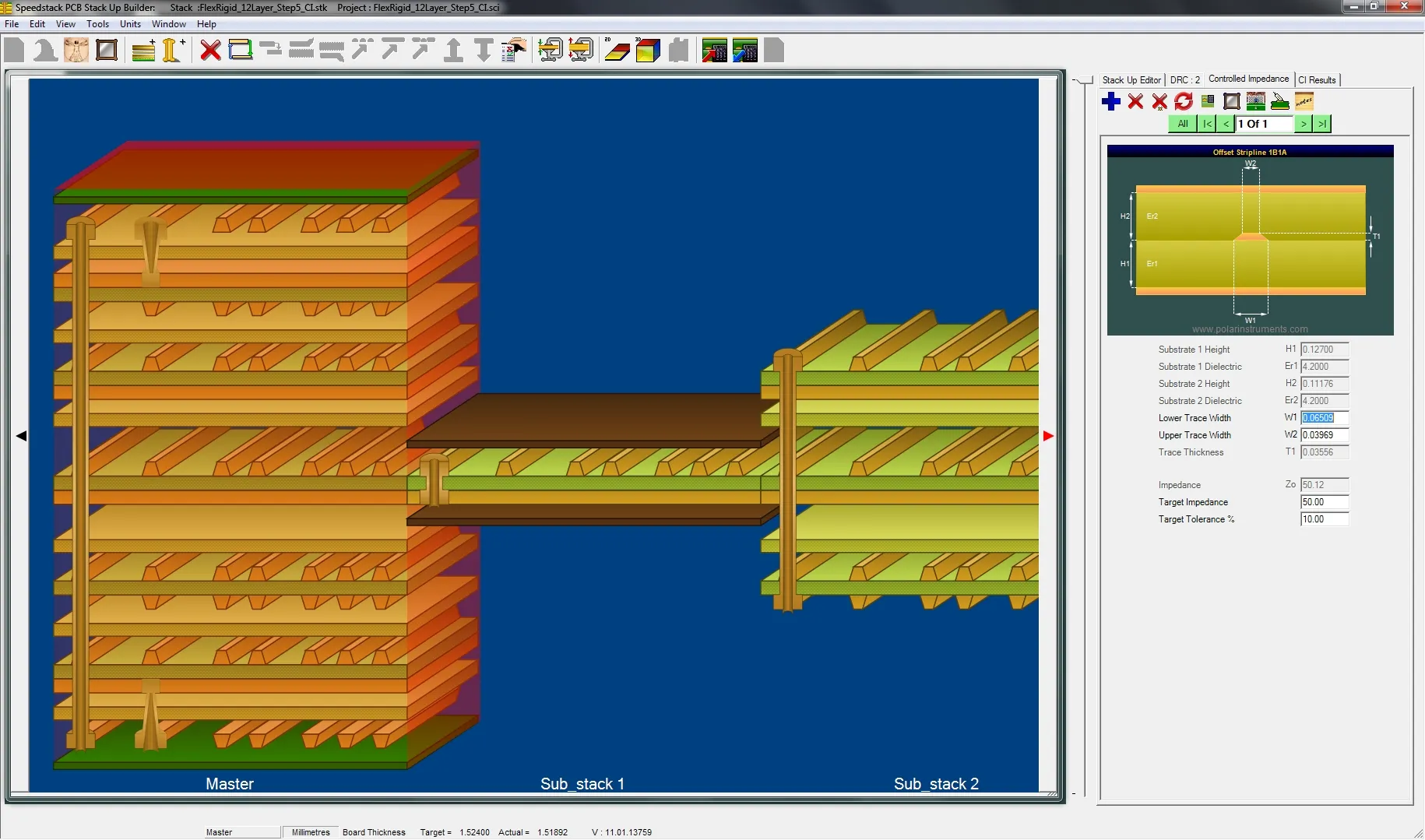
Semi-flex PCB design wearables starts with defining flex zones based on the device's mechanical requirements, typically 10-20% of the board area. Engineers use sectional stackups where a polyimide-based flex core sits between partially thinned FR4 rigid layers. Precise routing in flex areas avoids sharp bends, incorporating teardrop pads and curved traces to distribute strain evenly. Factory-driven simulations predict stress concentrations during repeated flexing, informing zone placement near hinges or straps. Component placement prioritizes rigid sections to prevent misalignment during bending. Adherence to IPC-2223 provides design rules for trace width, spacing, and overlap in transition regions.
The design process involves iterative modeling of bend radii aligned with the wearable's form factor. Flex zones require coverlay materials over exposed conductors for protection against abrasion. Rigid areas incorporate vias and planes for power integrity, ensuring signal integrity in high-frequency sensor circuits. Production feasibility demands balanced milling depths to avoid asymmetry-induced warpage. Engineers must account for assembly tolerances, as semi-flex boards demand specialized fixtures. This structured approach yields prototypes that transition smoothly from design to high-volume manufacturing.
Thermal management poses unique challenges, as flex materials exhibit different coefficients of thermal expansion than rigid substrates. Designers incorporate ground planes strategically to dissipate heat from processors without compromising flex performance. Solder mask selection focuses on flexibility in bend areas to prevent cracking. Overall, semi-flex PCB design wearables demands a holistic view of electrical, mechanical, and manufacturability factors.
Material Selection for Semi-Flex PCBs in Wearables
Semi-flex PCB material selection wearables hinges on combining durable rigid substrates with resilient flex dielectrics. FR4 serves as the rigid base for its mechanical strength and cost-effectiveness, while polyimide films provide the flex core due to superior thermal stability up to 260°C and low moisture absorption. Rolled annealed copper foils enhance ductility in dynamic flex zones, outperforming electrodeposited copper in bend cycles. Adhesives and coverlays must bond layers without delamination under humidity typical in sweat-exposed wearables. Factory testing verifies peel strength per industry norms to ensure layer integrity.
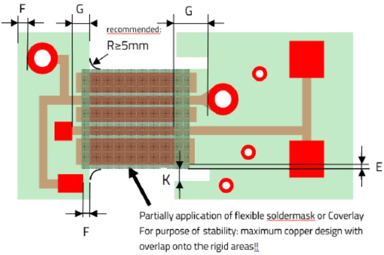
Coverlay materials, often acrylic or polyimide-based, protect traces in flex regions from environmental factors. Stiffeners, if needed, use polyimide reinforcements selectively to maintain flatness in rigid areas during assembly. Surface finishes like ENIG or OSP protect pads without hindering flex properties. Material compatibility extends to biocompatibility for skin-contact devices, prioritizing low outgassing. Engineers evaluate CTE mismatch to minimize stress at rigid-flex transitions.
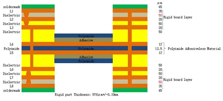
Selection criteria include dynamic vs. static flexing; wearables often demand semi-dynamic performance for wrist movements. Thinner flex layers, around 0.1-0.2 mm, enable tighter bends but require precise lamination control. Production scales favor materials with consistent dielectric constants for RF wearables like vital sign monitors.
Understanding Bending Limitations in Semi-Flex PCBs for Wearables
Semi-flex PCB bending limitations wearables arise from the controlled flex zones, restricting repeated deformation to avoid fatigue in rigid remnants. Designated flex areas, created by milling rigid layers to expose the flex core, tolerate specific radii determined by copper thickness and layer count. Exceeding these limits risks trace cracking or delamination, particularly in multilayer configurations. Factory qualification per IPC-6013 tests cyclic bending to establish endurance ratings. Engineers design with strain relief features like wider traces in transition zones.
Static bends, common in wearable straps, allow gentler curvatures over time, while dynamic applications limit cycles to prevent microcracks. Vibration from motion amplifies stress, necessitating reinforced anchors at zone edges. Production data highlights the importance of uniform milling depths for predictable behavior. Monitoring tools during prototyping reveal warpage tendencies post-bend.
Reliability improves by avoiding bends near vias or high-density areas. Guidelines recommend minimum flex zone lengths to distribute forces. Overall, respecting these limitations ensures long-term functionality in daily wear scenarios.
Achieving Miniaturization with Semi-Flex PCBs in Wearables
Semi-flex PCB miniaturization enables ultra-compact wearable designs by leveraging flex zones for 3D folding and rigid areas for high-density interconnects. Thinner profiles reduce overall volume, fitting sensors into sub-5 mm enclosures. Fine-line patterning in flex regions supports HDI features like microvias, shrinking footprints without sacrificing routing channels. Factory processes adapt laser drilling for precise vias in hybrid structures. This approach cuts assembly steps compared to wired rigid boards.
Challenges include maintaining impedance control across flex-rigid boundaries during miniaturization. Designers use blind vias and filled structures to optimize space. Flex tails connect to displays or batteries, eliminating bulky connectors. Production yields improve with panel-level processing for small boards.
Signal integrity benefits from shorter paths in folded layouts, crucial for low-power IoT wearables. Balancing density with bend reliability drives iterative DFM reviews.
Best Practices for Manufacturing Semi-Flex PCBs
Factory best practices start with precise depth milling using controlled CNC routing to define flex zones without damaging inner layers. Lamination sequences prioritize flex core bonding before rigid outer layers. Bake-out processes remove moisture to prevent voids. Solder mask application differentiates flex and rigid areas for optimal adhesion. Electrical testing includes continuity checks post-flex simulation.
Assembly requires low-stress soldering profiles to avoid warping. Fixtures secure boards during reflow, accommodating inherent flex. Inspection per IPC-A-600 verifies acceptability in bend regions. Scaling production involves statistical process control for milling uniformity. These steps ensure semi-flex boards meet wearable demands consistently.
Conclusion
Semi-flex PCBs strike an optimal balance for wearable tech, merging comfort through targeted flexibility with robust functionality in rigid zones. Key aspects like design rules, material choices, bending constraints, and miniaturization techniques empower engineers to create reliable devices. Factory-aligned standards guide production for repeatability. As wearables advance, semi-flex technology will drive further innovation in ergonomic electronics.
FAQs
Q1: What are the primary considerations in semi-flex PCB design wearables?
A1: Focus on defining flex zones via milling depths, ensuring strain relief at transitions, and placing components on rigid areas. Stackup symmetry prevents warpage, while trace routing follows curvature. Adhere to IPC-2223 for sectional guidelines. This approach supports compact, body-conforming layouts without reliability trade-offs.
Q2: How does semi-flex PCB material selection wearables impact performance?
A2: Polyimide cores offer thermal resilience and low CTE for flex zones, paired with FR4 rigid layers for strength. Ductile copper enhances bend endurance. Selection prioritizes biocompatibility and adhesion for sweat resistance. Factory testing confirms peel strength and dielectric properties.
Q3: What are common semi-flex PCB bending limitations wearables?
A3: Flex only in milled zones with radius tied to layer thickness; avoid dynamic overuse to prevent cracks. Static curves suit straps, dynamic for hinges. IPC-6013 qualification verifies cycles. Design reinforcements at edges extend life.
Q4: How does semi-flex PCB miniaturization benefit wearable devices?
A4: It enables 3D folding for volume reduction, HDI in rigid zones, and flex tails for connections. Shorter paths improve signals. Balances density with manufacturability for slim profiles.
References
IPC-2223C — Sectional Design Standard for Flexible/Rigid-Flexible Printed Boards. IPC.
IPC-6013D — Qualification and Performance Specification for Flexible and Rigid-Flex Printed Boards. IPC.
IPC-A-600K — Acceptability of Printed Boards. IPC.


