Introduction
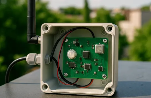
In industrial automation, sensor fusion represents a critical advancement for enhancing system reliability and decision-making capabilities. By integrating multiple sensors onto a single data acquisition PCB, engineers can achieve comprehensive environmental monitoring and precise control in harsh manufacturing environments. This approach combines data from diverse sources, such as temperature, pressure, and vibration sensors, to provide a unified view that surpasses the limitations of individual sensor outputs. Sensor interface design plays a pivotal role here, ensuring seamless communication between analog and digital sensors while maintaining signal integrity. As automation systems grow more complex, the demand for compact, efficient PCBs capable of handling multifaceted sensor inputs has surged. This article explores the intricacies of sensor fusion on industrial PCBs, offering insights into signal conditioning circuits, noise reduction for sensors, and best practices for robust integration.
What Is Sensor Fusion and Why It Matters in Industrial Automation
Sensor fusion involves the algorithmic and hardware-level combination of data from multiple sensors to produce more accurate, reliable, and comprehensive information than any single sensor could provide alone. In the context of a data acquisition PCB, it enables real-time processing of heterogeneous signals, which is essential for applications like predictive maintenance, robotics, and process control. For electric engineers designing industrial systems, understanding sensor fusion means recognizing its ability to mitigate individual sensor weaknesses, such as drift in analog thermistors or quantization errors in digital encoders. The relevance intensifies in environments with electromagnetic interference or mechanical vibrations, where fused data ensures operational continuity.
The industrial automation sector benefits immensely from this integration due to reduced wiring complexity and lower costs associated with fewer PCBs. A well-designed sensor interface design on a single board minimizes latency in data transmission, crucial for closed-loop control systems. Moreover, integrating analog and digital sensors fosters scalability, allowing systems to evolve without major redesigns. Noise reduction for sensors becomes a key factor, as poor fusion can amplify errors leading to faulty decisions. Ultimately, sensor fusion elevates PCB performance, aligning with the push for Industry 4.0 smart factories where data-driven insights drive efficiency.
Core Technical Principles of Sensor Fusion on PCBs
At the heart of sensor fusion lies effective sensor interface design, which bridges the gap between raw sensor outputs and the microcontroller or processor handling the data. Analog sensors, like thermocouples or strain gauges, produce continuous voltage signals that require amplification and filtering before digitization. Digital sensors, such as I2C accelerometers, output serialized data that demands precise timing protocols to avoid bus collisions. Integrating analog and digital sensors on the same PCB necessitates careful partitioning to prevent digital noise from corrupting analog paths. Signal conditioning circuits form the backbone, incorporating operational amplifiers for gain adjustment and low-pass filters to attenuate high-frequency noise.
Signal conditioning circuits must be tailored to sensor specifications, ensuring that weak signals from piezoelectric vibration sensors are boosted without introducing distortion. For instance, instrumentation amplifiers provide high common-mode rejection, vital in noisy industrial settings. Noise reduction for sensors involves strategic placement of decoupling capacitors near power pins and ground planes to stabilize voltage rails. Ferrite beads on signal lines further suppress electromagnetic interference. These elements collectively enable clean data acquisition PCB operation, where fused outputs reflect true environmental conditions rather than artifacts.
Power management emerges as another principle, with multiple sensors drawing varied currents that can cause droops if not isolated properly. Voltage regulators, both linear and switching types, distribute stable supplies while minimizing crosstalk. Thermal considerations influence layout, as heat from power circuits can affect sensor accuracy. Adherence to IPC-6012 standards for rigid printed boards ensures the PCB substrate supports high-density routing without warpage under thermal stress. This foundation allows fusion algorithms, running on embedded processors, to apply Kalman filters or complementary methods for optimal data blending.
Data synchronization poses a challenge in sensor fusion, requiring hardware timestamps or shared clocks to align readings from disparate sensors. Phase-locked loops synchronize digital interfaces, while analog-to-digital converters sample at rates matching sensor bandwidths. Oversampling techniques enhance resolution for low-frequency signals, reducing quantization noise. Integrating analog and digital sensors benefits from mixed-signal ICs that embed ADCs with programmable gain, streamlining the data acquisition PCB. Noise reduction for sensors extends to shielding, where guarded traces prevent capacitive coupling between adjacent lines.
Practical Solutions and Best Practices for Implementation
When designing a data acquisition PCB for sensor fusion, start with a layered stackup that dedicates inner planes to analog ground and digital ground, stitched together at multiple points to form a low-impedance return path. This separation is crucial for noise reduction for sensors, as digital switching transients can couple into analog sections via shared power planes. Route analog signals on dedicated layers, keeping them short and away from high-speed digital buses. Signal conditioning circuits should employ precision resistors and capacitors with tight tolerances to maintain calibration over temperature swings.
Component selection focuses on low-noise op-amps and ADCs with high signal-to-noise ratios, ensuring the dynamic range covers expected sensor outputs. For integrating analog and digital sensors, use multiplexers to share ADC channels efficiently, reducing pin count on the processor. Implement watchdog timers and error-checking protocols like CRC for digital communications to detect fusion anomalies. PCB layout software aids in simulating crosstalk, but physical prototyping validates performance. Compliance with J-STD-001 requirements for soldered electrical assemblies guarantees reliable connections under vibration.
Testing regimes include functional verification of each sensor interface design followed by integrated fusion tests under simulated industrial loads. Inject noise via conducted susceptibility tests to quantify signal conditioning circuits' effectiveness. Thermal cycling assesses long-term stability, aligning with IPC-A-610 acceptability criteria for class 3 assemblies. Firmware development incorporates sensor health monitoring, flagging degraded units to prevent skewed fusion data. These practices yield robust systems resilient to real-world stressors.
Firmware plays a pivotal role in realizing sensor fusion benefits, with interrupts prioritized for time-critical sensors like proximity detectors. Data preprocessing on the PCB, such as averaging or outlier rejection, lightens the load on host controllers. Calibration routines, stored in non-volatile memory, compensate for sensor offsets during power-up. Integrating analog and digital sensors shines in edge computing scenarios, where local fusion reduces bandwidth needs for networked systems.
Common Challenges and Troubleshooting Insights
One prevalent challenge in sensor fusion is ground bounce, where rapid current changes in digital grounds induce voltage spikes affecting analog precision. Mitigate this by adding ferrite chokes and RC snubbers at ground vias. Clock skew between digital sensors can desynchronize data; buffer clocks with zero-delay drivers to align edges. Electromagnetic compatibility issues arise from unshielded cables; conformal coatings on the PCB enhance protection without altering performance.
Troubleshooting begins with oscilloscope captures of sensor outputs pre- and post-conditioning to isolate noise sources. Spectrum analysis pinpoints frequencies for targeted filtering in signal conditioning circuits. If fusion outputs drift, verify power supply ripple below 1% of sensor excitation voltage. Mechanical stresses from mounting can warp the PCB, impacting trace integrity; reinforce with standoffs per IPC guidelines. These systematic approaches restore reliability efficiently.
Conclusion
Sensor fusion on a single industrial automation PCB transforms data acquisition from fragmented to holistic, empowering electric engineers with actionable intelligence. Key to success are meticulous sensor interface design, robust signal conditioning circuits, and proactive noise reduction for sensors. Integrating analog and digital sensors demands disciplined layout and adherence to standards like IPC-6012 and J-STD-001. By following these principles and practices, designers achieve compact, high-performance boards that drive automation excellence. Future advancements will likely emphasize AI-enhanced fusion, but solid hardware foundations remain paramount.
FAQs
Q1: What role does sensor interface design play in integrating analog and digital sensors on a data acquisition PCB?
A1: Sensor interface design ensures compatibility by providing level shifting, protocol handling, and isolation between analog voltage signals and digital serial buses. It includes buffers to prevent loading effects and multiplexers for efficient channel sharing. Proper design minimizes latency and supports real-time fusion, crucial for industrial control loops. Noise isolation through separate grounds enhances overall accuracy.
Q2: How can engineers implement noise reduction for sensors in signal conditioning circuits?
A2: Noise reduction for sensors starts with active filters using op-amps to attenuate unwanted frequencies while preserving signal bandwidth. Decoupling capacitors near each sensor pin stabilize supplies, and ground planes provide low-impedance returns. Shielded traces and ferrite beads block EMI ingress. Testing under load confirms effectiveness, ensuring clean data for fusion algorithms.
Q3: Why is a dedicated data acquisition PCB essential for industrial sensor fusion?
A3: A data acquisition PCB centralizes processing, reducing cabling and synchronization issues inherent in distributed setups. It enables optimized signal conditioning circuits tailored to multiple sensors, improving fusion quality. Compact integration lowers costs and enhances reliability in vibration-prone environments. Scalability supports adding sensors without system redesign.
Q4: What best practices ensure reliable integrating analog and digital sensors?
A4: Partition the PCB into analog and digital zones with stitched grounds to curb crosstalk. Use precision components in signal paths and validate with EMI scans. Firmware handles data alignment via timestamps. Adhere to soldering standards for durable joints under thermal cycling.
References
IPC-6012E — Qualification and Performance Specification for Rigid Printed Boards. IPC, 2018
J-STD-001H — Requirements for Soldered Electrical and Electronic Assemblies. IPC, 2018
IPC-A-610H — Acceptability of Electronic Assemblies. IPC, 2019


