Introduction
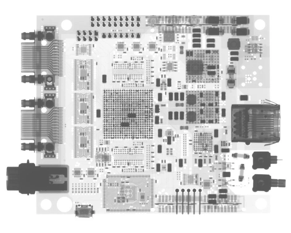
CT scanners produce detailed cross-sectional images by detecting X-rays that pass through the body, generating weak analog signals from detector arrays. These signals require precise signal conditioning on the printed circuit board (PCB) to ensure high-fidelity data for reconstruction algorithms. In CT scanner PCB design, signal conditioning encompasses amplification, filtering, impedance matching, noise reduction, data acquisition preparation, analog-to-digital conversion (ADC) interfacing, isolation, and protection circuits. Poor implementation leads to image artifacts, reduced resolution, or system failures in clinical settings. Engineers must prioritize these elements to meet stringent performance demands. This article explores the engineering principles and best practices for effective signal conditioning in such high-stakes applications.
What Is Signal Conditioning and Why It Matters in CT Scanner PCBs
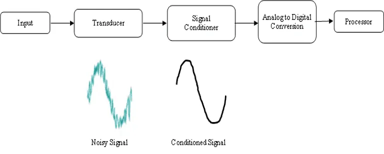
Signal conditioning refers to the process of modifying raw analog signals from sensors to make them suitable for further processing, particularly for data acquisition and analog-to-digital conversion. In CT scanners, photodiodes or scintillator-coupled detectors output microvolt-level signals with high dynamic range, susceptible to electromagnetic interference (EMI) and thermal noise. Without proper amplification and filtering, these signals degrade, compromising diagnostic accuracy. Impedance matching ensures efficient power transfer and minimizes reflections in high-frequency paths. Noise reduction techniques preserve signal integrity across the PCB, while isolation and protection circuits safeguard against patient safety risks and electrical faults. Ultimately, robust signal conditioning directly impacts scan speed, image quality, and compliance with medical reliability standards.
The relevance intensifies in CT systems due to rotational gantry speeds exceeding 0.3 seconds per rotation, demanding real-time processing of thousands of channels. Data acquisition systems sample at rates above 100 MSPS, amplifying the need for low-latency conditioning. Engineers overlook this at their peril, as even minor distortions propagate through reconstruction, yielding blurred or noisy images. Standards like IPC-2221 guide PCB layout to support these functions, emphasizing controlled impedance and minimal crosstalk.
Core Principles of Signal Conditioning in CT PCB Design
Amplification forms the first stage, using operational amplifiers to boost weak detector signals to ADC-compatible levels, typically 1-5 Vpp. Low-noise amplifiers (LNAs) with input-referred noise below 1 nV/√Hz are essential to avoid degrading the signal-to-noise ratio (SNR). Gain distribution across multi-stage designs prevents overload in high-signal events, such as dense bone regions. Feedback networks stabilize gain and bandwidth, tailored to the detector's frequency response up to several MHz.
Filtering eliminates unwanted frequencies, with anti-aliasing low-pass filters critical before ADC to prevent spectral folding. High-pass filters remove DC offsets from scintillator dark current, while notch filters target 50/60 Hz power line interference. Analog implementations using RC networks or active filters on the PCB offer sharp roll-offs, complementing digital post-processing. Proper filter design considers group delay to maintain temporal alignment across detector channels.
Impedance matching aligns source, transmission line, and load impedances, usually 50 or 100 ohms, to maximize signal power and reduce standing waves. In CT PCBs, differential pairs for high-speed signals require precise trace geometry per design guidelines. Mismatches cause ringing and attenuation, particularly at gigabit data rates for serialized outputs. Simulation verifies matching before fabrication.
Noise reduction demands holistic PCB strategies, including ground planes, via stitching, and partitioned analog-digital sections. Shielding cans enclose sensitive amplifiers, while decoupling capacitors suppress supply ripple. Thermal management prevents drift in precision components, ensuring consistent performance over continuous operation.
Data Acquisition and Analog-to-Digital Conversion Interfaces
Data acquisition in CT involves multiplexing hundreds of conditioned channels into fewer high-speed ADCs. Sample-and-hold circuits preserve signal amplitude during multiplexing, minimizing aperture errors. Clock distribution with low-jitter sources synchronizes sampling across the array.
Analog-to-digital conversion demands 14-16 bit resolution for 80-100 dB dynamic range, interfacing via parallel LVDS or serial JESD204B links. PCB routing preserves signal integrity with length-matched traces and controlled rise times. Transition regions use buffers to isolate analog front-ends from digital noise.
Isolation via transformers or optocouplers provides galvanic separation between detector and processing sections, complying with safety requirements. This prevents ground loops and fault propagation, crucial in patient-contacting systems.
Protection circuits employ TVS diodes, fuses, and clamps to guard against ESD, surges, and overvoltages. Resettable fuses allow recovery without replacement, while crowbar circuits limit currents during faults.
Best Practices for Implementing Signal Conditioning on CT Scanner PCBs
Component selection prioritizes low-noise, high-linearity parts with matched pairs for multi-channel consistency. Surface-mount precision resistors and capacitors ensure thermal stability, with values chosen via SPICE modeling.
PCB stackup features dedicated analog layers separated by ground planes from digital sections. Via fences and moats enhance isolation, while blind vias reduce stub inductance in high-density arrays. Trace widths and spacings follow IPC-A-600 guidelines for acceptability.
Routing strategies place amplifiers near detectors to minimize pickup, using guard traces around critical signals. Power distribution networks (PDNs) employ pi-filters for clean supplies, with ferrites blocking high-frequency noise.
Testing validates performance through vector network analysis for impedance and spectrum analysis for noise floor. Environmental stress screening per J-STD-020 simulates operational conditions, ensuring reliability.
Layout symmetry across detector channels prevents systematic errors, with fiducials aiding assembly precision. Firmware calibration compensates residual offsets post-assembly.
Common Challenges and Troubleshooting Insights
Electromagnetic interference from gantry motors couples into traces, addressed by twisted pairs and mu-metal shields. Crosstalk between adjacent channels requires increased spacing or differential signaling.
Thermal gradients cause gain drift, mitigated by heat spreaders and symmetric airflow paths. Vibration during rotation loosens connections, necessitating conformal coating and locking hardware.
Debugging employs oscilloscopes with low-noise probes to isolate issues, correlating time-domain glitches to frequency spectra. Simulation-PCB correlation refines designs iteratively.
Conclusion
Signal conditioning stands as the linchpin of CT scanner PCB design, integrating amplification, filtering, impedance matching, noise reduction, data acquisition, analog-to-digital conversion, isolation, and protection circuits into a cohesive system. Engineers achieve superior image quality by adhering to structured principles and best practices, guided by standards like IPC-2221 and IPC-A-600. Prioritizing these elements ensures reliable performance in demanding clinical environments. Future advancements in materials and integration will further elevate capabilities, but foundational engineering remains paramount.
FAQs
Q1: What role does amplification play in signal conditioning for CT scanner PCBs?
A1: Amplification boosts weak detector signals to levels suitable for data acquisition and analog-to-digital conversion, using low-noise op-amps to preserve SNR. Multi-stage designs distribute gain, preventing saturation during high-intensity scans. Proper feedback ensures bandwidth matching to detector response, critical for high-speed imaging. This step sets the foundation for downstream filtering and noise reduction.
Q2: How can engineers achieve effective noise reduction in CT PCB signal conditioning?
A2: Noise reduction involves partitioned layouts, ground planes, and shielding to isolate analog paths from digital noise. Decoupling capacitors and ferrites clean power supplies, while guard traces minimize capacitive coupling. Thermal stabilization prevents drift, ensuring consistent performance. These techniques maintain high SNR essential for diagnostic accuracy.
Q3: Why is impedance matching vital in CT scanner PCB design for signal conditioning?
A3: Impedance matching prevents reflections and signal loss in high-frequency paths, optimizing power transfer from amplifiers to ADCs. Differential pairs with controlled geometries achieve 50-ohm characteristic impedance. This reduces ringing and preserves waveform integrity during data acquisition. Verification through simulation ensures compliance across channels.
Q4: What protection circuits are essential in signal conditioning for medical PCBs like CT scanners?
A4: Protection circuits include TVS diodes for ESD, fuses for overcurrent, and clamps for surges, isolating sensitive amplification and filtering stages. Galvanic isolation via optocouplers enhances safety. These safeguard against faults without compromising signal fidelity. Resettable elements support field maintenance.
References
IPC-2221B — Generic Standard on Printed Board Design. IPC, 2012
IPC-A-600K — Acceptability of Printed Boards. IPC, 2020
J-STD-020E — Moisture/Reflow Sensitivity Classification. JEDEC, 2014


