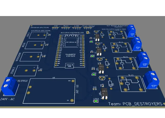
Introduction
Smart home devices have transformed everyday living with seamless connectivity through protocols like Wi-Fi 6 and Ethernet. These systems demand high-speed data transmission rates exceeding 1 Gbps in compact form factors such as hubs, cameras, and sensors. Signal integrity PCB design becomes critical as faster signals amplify vulnerabilities like reflections and noise in printed circuit boards. Poor signal integrity leads to data errors, reduced reliability, and compliance failures in densely packed layouts. Engineers face unique pressures in balancing performance, size, and cost for these consumer products. This article explores key challenges and proven strategies for high speed PCB layout in smart home applications.
Understanding Signal Integrity in High-Speed PCBs
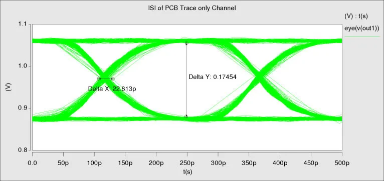
Signal integrity refers to the preservation of electrical signal quality from source to receiver without distortion or loss. In high-speed smart home device PCBs, signals propagate as transmission lines where mismatches cause reflections, attenuating waveforms. Key metrics include eye diagram quality, jitter, and bit error rates, all degrading with rising frequencies above 1 GHz. Why does it matter? Failed signal integrity results in intermittent connectivity, higher return rates, and regulatory hurdles for certification. For electric engineers, mastering signal integrity PCB design ensures robust performance amid shrinking geometries and multilayer stackups.
Core Causes of Signal Integrity Degradation
Reflections arise from impedance discontinuities at vias, bends, or connectors, violating transmission line principles. At high speeds, these mismatches create standing waves, peaking voltage swings beyond component tolerances. Crosstalk PCB issues emerge when aggressive coupling between adjacent traces induces noise on victim lines, especially in parallel routing. Ground bounce and power supply noise further couple through shared planes, exacerbating problems in power-sensitive smart devices. Dielectric losses increase with frequency due to material tan delta, while skin effect confines currents to trace surfaces, raising resistance. Engineers must model these mechanisms using field solvers to predict behaviors pre-layout.
Crosstalk and Its Impact on High-Speed Layouts
Crosstalk divides into capacitive and inductive types, with mutual inductance dominating at gigabit speeds. In high speed PCB layout, near-end and far-end crosstalk distort timing margins, closing eye openings. Compact smart home boards with tight trace spacing under 5 mils intensify this, as edge-coupled microstrips couple up to 10% of aggressor voltage. Return paths through split planes fragment ground, boosting common-mode noise. Simulations reveal peak crosstalk scales with trace length and separation, demanding spacing rules like 3W for differential pairs. Proactive spacing and guard traces mitigate risks without excessive layer counts.
EMI Challenges in Dense Smart Home PCBs
Electromagnetic interference (EMI) plagues high-speed designs as radiating traces act as antennas above 100 MHz. EMI reduction PCB strategies counter both radiated and conducted emissions from clock lines and data buses. In smart home devices, regulatory limits like FCC Class B tighten requirements for residential environments. Poor return current paths spread magnetic fields, while impedance mismatches radiate harmonics. Board-edge effects and cavity resonances in enclosures amplify fields, failing pre-compliance scans. Layer sequencing with solid ground planes adjacent to signal layers suppresses emissions effectively.
Impedance Matching Techniques for Reliable Performance
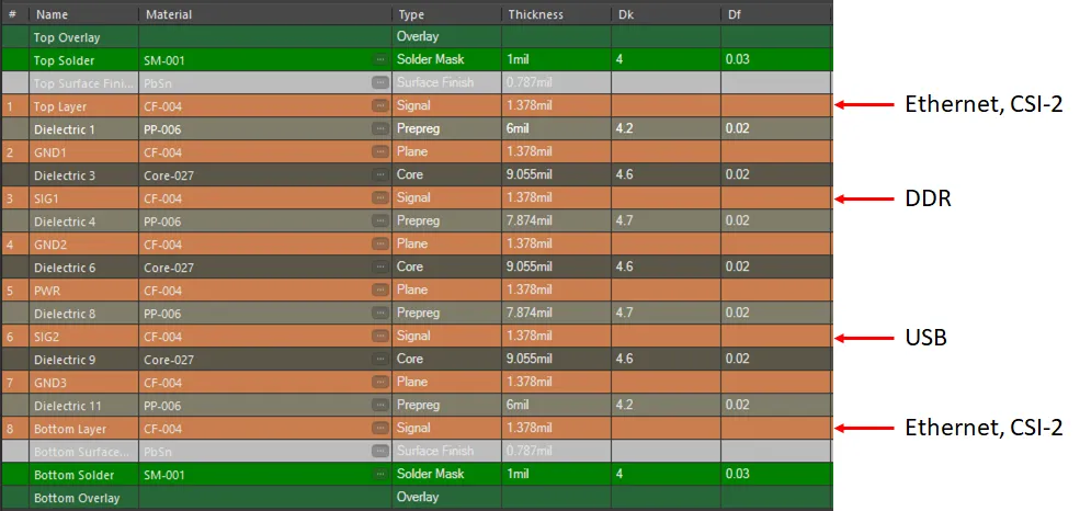
Controlled impedance ensures maximum power transfer, minimizing reflections per transmission line theory. Impedance matching techniques include precise trace width calculations based on stackup parameters like dielectric height and Er. For 100-ohm differential pairs common in Ethernet, widths around 4-6 mils on 1.6 mm FR-4 suit outer layers. Vias demand back-drilling or stub removal to avoid stubs longer than 1/10 wavelength. T-section or tapered transitions smooth discontinuities at connectors. Field solvers verify Z0 within 10% tolerance, aligning with IPC-2221 guidelines for high-speed design.
IPC-2221 establishes generic requirements for conductor sizing and spacing to maintain signal integrity.
Best Practices for High-Speed PCB Layout
Start with stackup optimization, placing high-speed signals on inner layers between power and ground planes for confinement. Length tuning equalizes pair delays within 0.5 mil for DDR or PCIe interfaces in smart hubs. Orthogonal routing perpendicular to adjacent layers reduces broadside coupling in crosstalk PCB scenarios. Decoupling capacitors near IC pins shunt high-frequency noise, stabilizing supplies. Serpentine patterns for length matching preserve impedance if bends exceed 2W radius. Post-layout extraction feeds SI simulations, iterating until passing eye masks.
Mitigating Losses and Timing Skew
Conductor losses from skin effect demand wider traces or copper thickness above 1 oz/ft2 at multi-GHz. Dielectric absorption in low-cost laminates distorts pulses, favoring lower-loss materials per performance specs. Skew between differential pairs arises from unequal lengths or etch variations, timing out receivers. Matched routing with meanders and phase-aligned vias corrects this. Via fences or stitching grounds every lambda/20 shield slots. Thermal management prevents CTE mismatches warping boards, impacting high speed contacts.
EMI Reduction PCB Techniques in Practice
Dedicated ground pours under noisy traces absorb return currents, cutting loop areas. Via shielding encircles sensitive nets, shunting fields to planes. Spread-spectrum clocking dithers harmonics below EMI limits. Filtered connectors with common-mode chokes block conducted paths. Enclosure grounding ties chassis to PCB grounds via multiple points. These align with IPC-6012 performance classes for high-reliability boards.
IPC-6012 defines qualification specs ensuring dimensional stability critical for impedance control.
Advanced Troubleshooting for Smart Home Designs
Engineers debug SI failures using TDR oscilloscopes to pinpoint impedance bumps. VNA sweeps quantify S-parameters for insertion loss and return loss. Near-field probes map EMI hotspots pre-shielding. Fabricating test coupons on panel edges validates stackup models. Iterative prototypes refine rules, as simulations overlook fab tolerances. J-STD-001 assembly standards guide soldering to avoid cold joints distorting parasitics.
J-STD-001 outlines requirements for soldered electrical assemblies, influencing high-speed interconnect reliability.
Conclusion
Signal integrity PCB design demands holistic attention from stackup to assembly in high-speed smart home devices. Mastering impedance matching techniques, crosstalk PCB mitigation, and EMI reduction PCB methods ensures gigabit performance without errors. Logical layout rules grounded in transmission theory yield predictable outcomes. Adhering to standards like IPC guidelines elevates designs from functional to robust. Electric engineers benefit from simulations and test vehicles to navigate these challenges efficiently. Future protocols will intensify these needs, rewarding proactive strategies today.
FAQs
Q1: What are the primary causes of crosstalk PCB in high speed PCB layout?
A1: Crosstalk stems from capacitive and inductive coupling between parallel traces, worsening with proximity and length. In smart home PCBs, tight spacing under 100 microns induces voltage glitches on victim lines. Orthogonal routing and increased separation by 3-5 times trace width reduce it effectively. Ground planes between layers further isolate signals. Simulations predict levels before fabrication.
Q2: How do impedance matching techniques improve signal integrity PCB design?
A2: Impedance matching prevents reflections by matching trace Z0 to driver and receiver specs, typically 50 or 100 ohms. Techniques include width adjustments via stackup calculators and via optimization like back-drilling. Tolerance under 10% opens eye diagrams at high speeds. Field solvers confirm designs pre-layout. This is essential for reliable data in smart devices.
Q3: What EMI reduction PCB strategies work best for compact smart home boards?
A3: Solid ground planes adjacent to signal layers confine fields, while via stitching every 1/20 wavelength blocks slots. Guard traces and decoupling suppress noise coupling. Spread-spectrum clocks diffuse peaks. These maintain compliance in dense layouts without added cost. Pre-compliance scans validate efficacy.
Q4: Why is high speed PCB layout critical for smart home device performance?
A4: High-speed layouts handle multi-Gbps rates in Wi-Fi and Ethernet, where SI failures cause packet loss and latency. Proper routing, matching, and shielding preserve waveform integrity. Compact sizes amplify crosstalk and EMI risks. Standards-guided practices ensure reliability. Engineers prioritize simulations for first-pass success.
References
IPC-2221B — Generic Standard on Printed Board Design. IPC, 2012
IPC-6012E — Qualification and Performance Specification for Rigid Printed Boards. IPC, 2017
J-STD-001H — Requirements for Soldered Electrical and Electronic Assemblies. IPC, 2020


