Introduction
High-frequency designs in RF, microwave, and 5G/6G systems demand materials that preserve signal fidelity over long traces and at multi-GHz speeds. PTFE PCBs deliver exactly that advantage through their ultra-low dielectric constant (Dk ≈ 2.1–2.5) and dissipation factor (Df < 0.0005), making them the material of choice for applications where even a few dB of signal loss PTFE PCB can render a channel unusable. Engineers focused on PTFE PCB signal integrity and PTFE high frequency loss minimization must master every variable—from copper roughness and stack-up symmetry to via transitions—to keep eye diagrams open and bit-error rates below 10⁻¹².This guide distills factory-proven techniques and data-backed strategies for achieving industry-leading performance.
Understanding PTFE PCBs and the Importance of Signal Integrity
PTFE (polytetrafluoroethylene) serves as the core dielectric in high-frequency laminates because it maintains a stable Dk across a wide frequency band and exhibits the lowest loss tangent among common PCB materials. Unlike FR-4, whose Dk drifts and Df rises sharply above 1 GHz, PTFE keeps phase distortion and energy dissipation to a minimum. This directly combats signal loss PTFE PCB and supports PTFE PCB signal integrity in systems operating beyond 10 Gbps or 5 GHz.
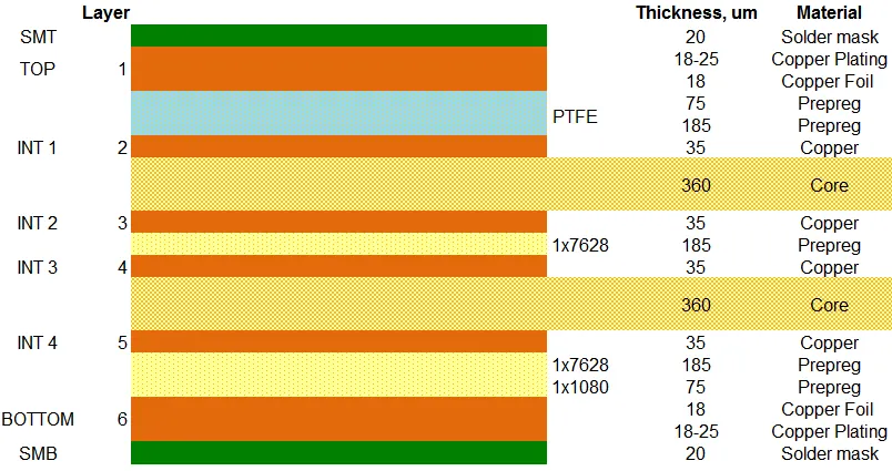
Signal integrity encompasses amplitude preservation, rise-time fidelity, and timing accuracy from transmitter to receiver. In PTFE boards, poor integrity appears as overshoot, ringing, inter-symbol interference, or closed eye diagrams. The consequences are measurable: higher bit-error rates, increased jitter, and reduced system margin. Factory processes for PTFE PCBs therefore emphasize precision etching, vacuum lamination to eliminate voids, and tight thickness control (±0.001 in) to guarantee repeatable electrical performance.
Dk & Df Comparison at 10 GHz
| Material | Dielectric Constant (Dk) | Dissipation Factor (Df) | Typical Insertion Loss (dB/in) | Best-Use Case |
|---|---|---|---|---|
| PTFE (pure) | 2.1 | 0.0002 | 0.15–0.25 | mmWave, satellite, radar |
| Rogers RO4350B | 3.48 | 0.0037 | 0.45–0.60 | 5G base stations |
| FR-4 (standard) | 4.3–4.6 | 0.018–0.025 | 1.2–1.8 | Digital < 2 GHz |
The data clearly shows why PTFE is preferred when every tenth of a dB counts.
Mechanisms of Signal Loss in PTFE PCBs
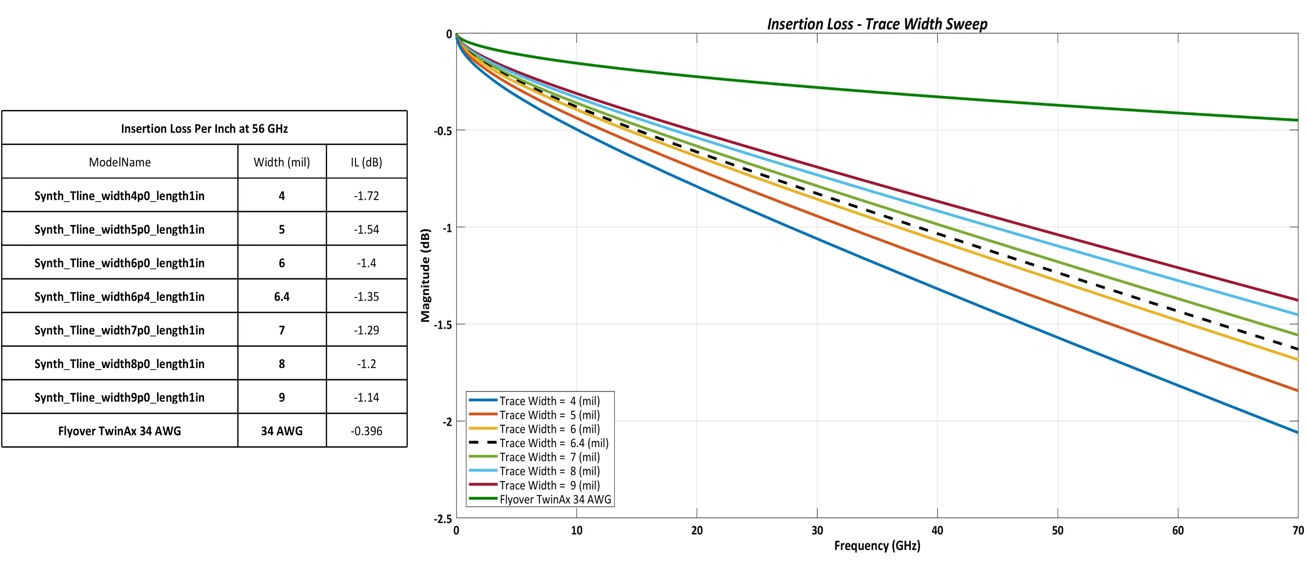
Signal loss PTFE PCB arises from two dominant mechanisms: dielectric absorption and conductor attenuation. Dielectric loss scales with frequency squared and is governed by the material’s loss tangent; PTFE’s exceptionally low Df keeps this contribution minimal. Conductor loss, however, becomes dominant above ~5 GHz due to the skin effect, where current crowds to the copper surface, and roughness scattering, which increases effective resistance.
Skin-Effect & Copper Roughness Subsection
At microwave frequencies, current flows within ~1–2 μm of the conductor surface (skin depth δ ≈ 0.66 / √f μm at 10 GHz). Rough copper foils (RMS roughness > 1 μm) scatter electrons, raising attenuation by 15–30% versus smooth electrodeposited (ED) or rolled annealed (RA) foils. Low-profile copper (VLP or HVLP, RMS < 0.4 μm) is therefore standard for PTFE high frequency loss minimization.
Additional contributors include surface contamination, plating voids, and fiber weave in reinforced PTFE composites. Full-channel simulations that incorporate these effects allow engineers to budget loss accurately and select the right foil type before tape-out.
Related Reading: Exploring the Material Properties of PTFE PCBs: Dielectric Constant, Loss Tangent, and Thermal Stability
Achieving PTFE PCB Impedance Matching
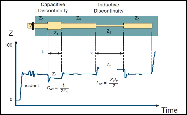
PTFE PCB impedance matching prevents reflections that distort waveforms and amplify noise. Characteristic impedance (Z₀) is a function of trace width, dielectric height, and PTFE’s low Dk—allowing wider traces for the same 50 Ω target compared with FR-4. Mismatches arise from etch tolerances (±0.0005 in typical), thickness variation, or asymmetric stack-ups.
Best-practice simulation uses 2.5D or 3D field solvers (HFSS, SIwave) that include actual copper roughness models and frequency-dependent Dk/Df. Engineers specify test coupons at the operational frequency band and require fabricators to deliver TDR-verified impedance within ±5%. Symmetric stripline builds with tightly coupled reference planes further stabilize Z₀ against fab drift. Differential pairs require even/odd-mode matching to maintain balance.
IPC-6012 qualification coupons and post-fab TDR reports close the
-to-fab loop, ensuring every channel meets the budgeted impedance window.
Mitigating PTFE PCB Crosstalk
PTFE PCB crosstalk couples energy between adjacent traces through capacitive, inductive, or mutual mechanisms. Even with PTFE’s low Dk, fringing fields remain significant at multi-GHz speeds. Near-end crosstalk (NEXT) peaks from backward waves; far-end crosstalk (FEXT) affects receiver timing.
3W/5W Rule Visuals & Practical Implementation
Apply a minimum 3× trace width (3W) spacing for single-ended signals and 5W for aggressive aggressor-victim pairs. Insert ground-plane stitching vias every λ/20 along parallel runs. Differential routing with tight intra-pair spacing and symmetric length matching cancels common-mode coupling. In multilayer boards, dedicate entire planes to ground between signal layers. These rules routinely reduce crosstalk below –40 dB at 10 GHz in PTFE constructions.
Best Practices for Design and Fabrication
Copper-Foil & Surface-Finish Section
Specify reverse-treated or very-low-profile copper foils (RMS roughness < 0.4 μm) to cut skin-effect loss. For surface finish, ENIG or immersion silver provide excellent solderability and minimal insertion-loss contribution; avoid HASL on high-frequency layers due to solder roughness.
Additional Best Practices
- Alternate signal and plane layers in symmetric stack-ups.
- Minimize via count; use blind/buried or back-drilled vias to eliminate stubs.
- Route parallel to the weave direction in glass-reinforced PTFE to avoid anisotropy.
- Perform full-channel simulation including connectors and packages.
- Require fabricators to supply insertion-loss and impedance test data per IPC-6012 coupon requirements.
Related Reading: The Ultimate Guide to PTFE PCB Stackup Design for Optimal Performance
PTFE vs. Alternative Low-Loss Materials
While PTFE offers the lowest loss, alternatives may suit specific cost or mechanical needs:
| Material | Dk (10 GHz) | Df (10 GHz) | Loss (dB/in @ 10 GHz) | Cost Factor | Processability | Typical Application |
|---|---|---|---|---|---|---|
| PTFE (pure) | 2.1 | 0.0002 | 0.15–0.25 | 4–6× | Moderate | mmWave, satellite |
| Rogers RO4350B | 3.48 | 0.0037 | 0.45–0.60 | 2–3× | Good | 5G infrastructure |
| Megtron 6 | 3.4 | 0.004 | 0.55–0.70 | 1.8× | Excellent | High-speed digital |
| FR-4 (low-loss) | 3.8–4.2 | 0.008–0.012 | 1.0–1.5 | 1× | Excellent | Cost-sensitive < 5 GHz |
PTFE remains the benchmark for the most demanding loss budgets; Rogers and Megtron strike a practical balance for many 5G and high-speed digital designs.
Troubleshooting Signal Integrity Issues
Unexpected loss spikes often trace to rough copper or micro-voids; TDR reveals etch undercuts. Elevated crosstalk points to missing ground referencing—add stitching vias every 1/20 λ. Closed eye diagrams after assembly frequently indicate via resonance; blind vias or back-drilling restore margin. Systematic VNA measurements correlated against simulation refine models and close the sim-to-hardware gap.
Advanced Techniques & Case Studies
In 28 GHz 5G phased-array antennas, 8–10 oz heavy-copper PTFE cores combined with HVLP foil and blind vias deliver < 0.3 dB/in loss while handling 20 W per element. Satellite Ka-band transceivers use pure PTFE with laser-drilled microvias to eliminate stub resonance, achieving 18-year mission life in GEO orbit. These real-world examples demonstrate how deliberate material, geometry, and process choices translate PTFE high frequency loss minimization into measurable system performance.
Conclusion
PTFE PCB signal integrity hinges on minimizing signal loss PTFE PCB through low-roughness copper, symmetric stack-ups, precise impedance control, and aggressive crosstalk mitigation. By applying the factory-proven techniques and data-backed comparisons in this guide, engineers can consistently achieve the performance required for next-generation RF, microwave, and high-speed digital systems. Standards such as IPC-4101, IPC-2221, and IPC-6012 provide the foundation, while early collaboration with qualified fabricators ensures repeatable results. The payoff is reliable, high-margin designs that power today’s—and tomorrow’s—most demanding applications.
FAQs
Q1: What primarily drives PTFE PCB signal loss at high frequencies?
A1: Dielectric dissipation (loss tangent) and conductor skin-effect/roughness scattering dominate. Low-profile copper and short, straight traces per IPC-2221 minimize signal loss PTFE PCB.
Q2: How do you maintain PTFE PCB impedance matching in multilayer boards?
A2: Use symmetric stripline builds, tight plane coupling, and TDR-verified coupons. Field solvers that incorporate actual copper roughness deliver accurate Z₀ predictions.
Q3: What spacing rules minimize PTFE PCB crosstalk?
A3: Apply 3W–5W separation, ground-plane shielding, and differential routing with length matching. These practices routinely keep coupling below –40 dB at 10 GHz.
Q4: Why is copper foil selection critical for PTFE high frequency loss minimization?
A4: Rough foils scatter electrons and increase skin-effect loss dramatically above 5 GHz. Very-low-profile (VLP) or rolled-annealed foils are the industry standard for microwave performance.
References
- IPC-4101 — Specification for Base Materials for Rigid and Multilayer Printed Boards. IPC.
- IPC-2221 — Generic Standard on Printed Board Design. IPC.
- IPC-6012E — Qualification and Performance Specification for Rigid Printed Boards. IPC.


