Introduction
Insulin pumps represent a critical advancement in diabetes management, delivering precise doses of insulin based on real-time sensor data and algorithmic control. The printed circuit board (PCB) at the heart of these devices handles sensitive analog signals from glucose sensors, digital commands for pump actuation, and possibly wireless communications. Signal integrity in insulin pump PCBs directly impacts the accuracy of insulin delivery, where even minor distortions can lead to over- or under-dosing with serious health consequences. Engineers must prioritize impedance control, careful signal routing, and protection against electromagnetic interference (EMI) to maintain reliable performance in a compact, battery-powered environment. This article explores the principles and best practices for achieving robust insulin pump PCB signal integrity, tailored for electrical engineers designing high-reliability medical electronics.
What Is Signal Integrity in Insulin Pump PCBs and Why It Matters
Signal integrity refers to the preservation of electrical signal quality as it travels across the PCB, free from distortions like reflections, noise, or attenuation. In insulin pump PCBs, this encompasses both analog paths for low-level sensor inputs and digital lines for microcontroller communications and motor drive signals. Poor signal integrity can cause timing errors in pump mechanisms or inaccurate glucose readings, compromising patient safety in life-sustaining applications. Factors such as trace impedance variations, crosstalk between adjacent signals, and EMI from the pump's mechanical components exacerbate these risks in dense layouts. Adhering to standards like IPC-2221 for design guidelines ensures consistent performance under varying thermal and mechanical stresses typical in wearable medical devices. Ultimately, strong signal integrity supports regulatory compliance and long-term reliability, enabling precise insulin delivery algorithms to function without interruption.
Key Challenges Affecting Insulin Pump PCB Signal Integrity
Insulin pump PCBs operate in challenging environments with mixed-signal designs, where high-impedance analog lines coexist with switching digital circuits. Reflections arise from impedance mismatches at vias, connectors, or terminations, leading to overshoot and ringing that degrade sensor accuracy. Crosstalk occurs when capacitive or inductive coupling between parallel traces induces noise, particularly problematic for glucose sensor signals operating at microvolt levels. EMI shielding becomes essential near the pump motor, which generates electromagnetic noise during operation, potentially coupling into sensitive control lines. Ground bounce and power supply noise further complicate matters in battery-constrained systems with limited decoupling space. These challenges demand a holistic approach to layout, materials, and verification to prevent cascading failures in insulin delivery timing.
Technical Principles of Impedance Control in Insulin Pump PCBs
Impedance control PCB design maintains consistent characteristic impedance along signal paths, typically 50 ohms single-ended or 100 ohms differential for digital interfaces. This is achieved by balancing trace width, dielectric thickness, and copper thickness, as guided by stackup calculations. In insulin pump applications, controlled impedance prevents signal reflections that could corrupt data packets or timing pulses essential for dose calculations. Variations in laminate dielectric constant due to manufacturing tolerances must stay within tight limits to avoid skew in multi-layer boards. Engineers calculate impedance using field solver approximations, considering reference plane proximity and via stubs. Proper impedance control PCB practices ensure high-fidelity signals, directly supporting accurate insulin pump PCB signal integrity.
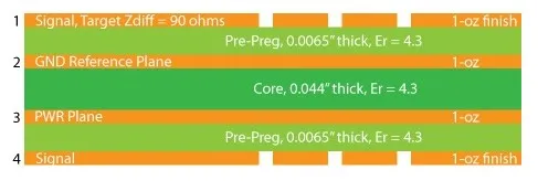
IPC-2141 provides foundational guidelines for controlled impedance in high-speed designs, adaptable to the moderate frequencies in medical PCBs. By specifying trace geometries relative to ground planes, it minimizes discontinuities that plague compact insulin pump layouts.
Signal Routing Techniques for Optimal Performance
Signal routing techniques form the backbone of crosstalk reduction in medical PCBs, starting with orthogonal routing between layers to minimize parallel run lengths. Differential pairs for sensor data maintain balance and reject common-mode noise, with length matching to within millimeters for clock signals. Avoid right-angle bends; use 45-degree mitered corners to reduce reflections and stub effects. Guard traces or ground pours between sensitive lines further isolate analog from digital domains. In insulin pump PCBs, route high-current motor drives away from sensors, using dedicated power planes to contain return currents. These signal routing techniques enhance overall signal integrity while fitting within the size constraints of portable devices.
Via optimization is crucial: blind or buried vias reduce stub lengths, preserving impedance continuity. Length-tuned meanders equalize propagation delays in bus structures, preventing bit errors in control firmware.
EMI Shielding Strategies in Insulin Pump PCB Design
EMI shielding PCB approaches begin with full ground planes on inner layers, providing low-inductance return paths and screening adjacent signals. Stitch vias along trace edges create Faraday cage effects, blocking motor-generated fields from reaching control circuitry. For external shielding, metal cans or conductive gaskets interface with the enclosure, grounded at multiple points to avoid slots. Component placement separates noisy elements like DC-DC converters from precision analog sections, with ferrite beads on power lines attenuating high-frequency noise. In battery-powered insulin pumps, these EMI shielding PCB methods comply with medical EMC requirements without excessive power draw. Layer sequencing, such as signal-ground-signal, symmetrically sandwiches traces to equalize fields and reduce radiation.
Crosstalk reduction in medical PCBs pairs well with shielding; increasing trace-to-trace spacing per IPC-2221 recommendations inversely scales coupling by the square of distance. This is vital for maintaining signal-to-noise ratios in glucose monitoring channels.
Best Practices for Implementation and Verification
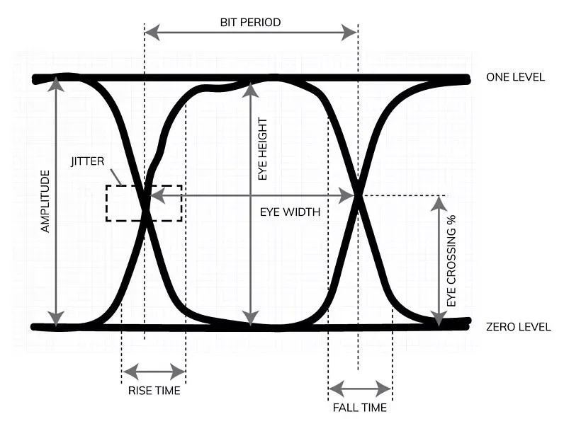
Start with a symmetric stackup for uniform impedance across layers, using low-loss dielectrics for analog sections. Simulate pre-layout with tools modeling S-parameters to predict reflections and crosstalk. During routing, enforce design rules for minimum clearances and enforce length matching. Post-layout extraction verifies eye diagrams and insertion loss, iterating if margins fall short. Fabrication tolerances demand spec sheets detailing impedance targets and test coupons on panels. For insulin pump PCB signal integrity, functional testing under vibration simulates wearables' stresses, confirming no intermittent failures.
Prototype builds include time-domain reflectometry (TDR) for impedance profiling and near-field probes for EMI hotspots. These steps bridge design to production, ensuring impedance control PCB reliability.
Troubleshooting Common Signal Integrity Issues
Engineers often encounter ringing in insulin pump prototypes from unterminated fast edges; add series resistors at drivers matching source impedance. Excessive crosstalk signals wideband noise on scopes; increase spacing or insert ground traces as shields. EMI pickup near motors shows periodic spurs; relocate traces or add shielding cans. Ground loops from split planes cause offsets in analog readings; unify returns with stitching. Power integrity ties in, with inadequate decoupling yielding jitter; distribute capacitors densely. Systematic debugging, from simulation to bench testing, resolves these for robust insulin pump PCB signal integrity.
A case insight from high-reliability designs reveals that 80% of issues stem from layout violations, underscoring early DRC enforcement.
Conclusion
Signal integrity in insulin pump PCBs demands meticulous attention to impedance control, signal routing techniques, EMI shielding, and crosstalk reduction to guarantee precise insulin delivery. By applying structured engineering principles and leveraging standards like IPC-2221 and IPC-2141, designers mitigate risks in mixed-signal environments. Practical implementation through simulation, verification, and troubleshooting ensures compliance and performance in life-critical applications. Electrical engineers can achieve this balance in compact form factors, advancing reliable medical electronics. Prioritizing these elements not only enhances device accuracy but also builds trust in wearable health technologies.
FAQs
Q1: What role does impedance control play in insulin pump PCB signal integrity?
A1: Impedance control maintains consistent trace characteristics to prevent reflections that distort timing-critical signals for insulin dosing. Engineers specify widths and stackups to match driver/receiver impedances, typically 50 ohms. This reduces overshoot and ensures data integrity from sensors to microcontrollers. Verification via TDR confirms tolerances during fabrication.
Q2: How can signal routing techniques reduce crosstalk in medical PCBs?
A2: Signal routing techniques like orthogonal layering and guard traces minimize parallel coupling, keeping noise below sensor thresholds. Differential pairs reject common-mode interference effectively. Maintain spacings per design rules to scale down capacitive effects. These practices enhance overall insulin pump PCB signal integrity in dense layouts.
Q3: Why is EMI shielding critical for insulin pump PCB design?
A3: EMI shielding PCB methods, such as ground planes and vias, block motor noise from corrupting control signals. This preserves low-level glucose data accuracy essential for delivery algorithms. Proper enclosure integration contains emissions without impacting battery life. Compliance avoids regulatory hurdles in medical devices.
Q4: What are best practices for crosstalk reduction in medical PCBs?
A4: Crosstalk reduction in medical PCBs involves wider trace spacing, ground stitching, and separating analog/digital zones. Avoid long parallel runs and use shielding layers. Simulations predict coupling levels pre-layout. These ensure reliable signal integrity for precise insulin pump operations.
References
IPC-2221B — Generic Standard on Printed Board Design. IPC, 2012
IPC-2141 — Design Guide for High-Speed Controlled Impedance Printed Boards. IPC, 1996
IPC-6012E — Qualification and Performance Specification for Rigid Printed Boards. IPC, 2017


