Introduction
In the realm of printed circuit board (PCB) design, ensuring the integrity of signal layers is paramount for achieving reliable performance in electronic systems. Signal layer testing forms the backbone of validating a PCB's ability to transmit data without degradation, especially in high-speed applications. For electrical engineers, understanding PCB testing methods, such as signal integrity testing, impedance testing, and TDR testing, is essential to prevent issues like crosstalk or signal loss. This article explores the critical role of signal layers in PCB design, delves into various testing methodologies, and provides practical insights into achieving optimal design performance. By adhering to widely recognized industry standards, engineers can ensure their designs meet stringent quality and reliability requirements in demanding environments.
What Are Signal Layers and Why Do They Matter
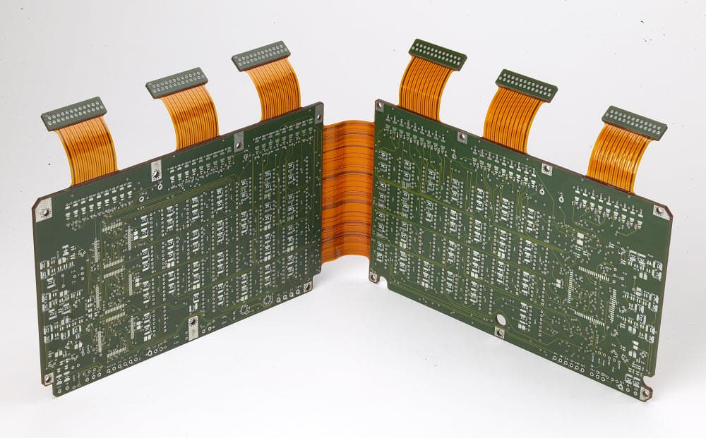
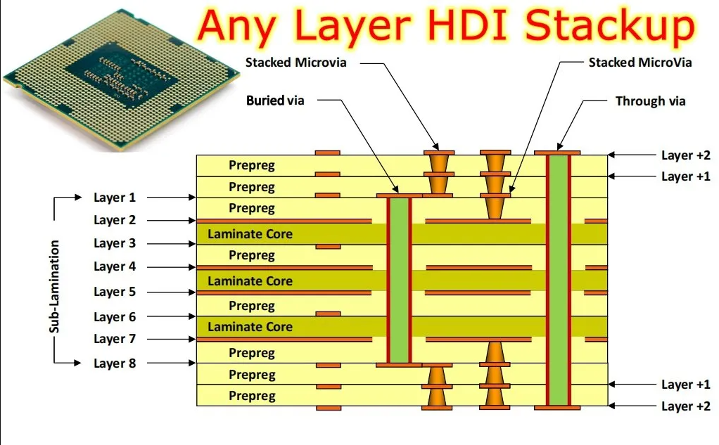
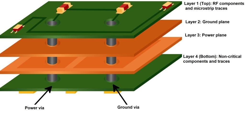
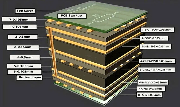
Signal layers in a PCB are dedicated copper layers used to route electrical signals between components. These layers are crucial in multilayer boards, where they are often sandwiched between ground and power planes to minimize interference. The performance of signal layers directly impacts the overall functionality of the circuit, particularly in high-frequency or high-speed designs where timing and signal clarity are critical.
The importance of signal layers cannot be overstated. Poorly designed or untested signal layers can lead to signal degradation, increased noise, or complete system failure. For instance, in applications like telecommunications or automotive electronics, even minor signal distortions can result in data errors or safety risks. Effective signal layer testing ensures that signals propagate as intended, maintaining the integrity of the design under various operating conditions. This process is vital for engineers aiming to deliver robust and reliable electronic products.
Related Reading: Signal Integrity PCB Designers
Technical Principles of Signal Layer Testing
Signal layer testing focuses on evaluating how well a PCB handles electrical signals without distortion or loss. Several key principles underpin this process, each addressing specific aspects of signal behavior.
Signal Integrity Testing
Signal integrity testing assesses the quality of a signal as it travels from transmitter to receiver. This involves analyzing factors like rise time, jitter, and noise margins. Poor signal integrity can result from reflections, crosstalk, or improper termination, all of which degrade performance. Testing often involves simulation tools and physical measurements to identify issues before production. Ensuring signal integrity is especially critical in high-speed digital designs where data rates exceed several gigabits per second.
Impedance Testing
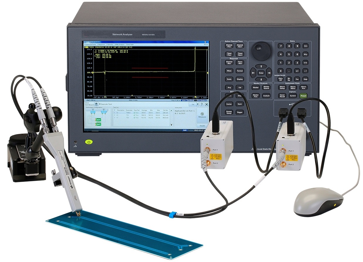
Impedance testing measures the opposition to alternating current in a signal path, ensuring it matches the design specifications. Mismatched impedance can cause signal reflections, leading to data errors. This testing typically uses precision instruments to verify that traces maintain consistent impedance across their length. Controlled impedance is a cornerstone of reliable signal transmission, particularly in applications involving differential pairs or high-frequency signals.
Time-Domain Reflectometry (TDR) Testing
TDR testing is a specialized method to locate discontinuities or faults in a signal path. By sending a short pulse down a trace and measuring the reflected signal, engineers can pinpoint impedance mismatches or breaks. TDR testing is invaluable for diagnosing issues in long traces or complex multilayer boards. It provides a clear picture of where signal integrity might be compromised, allowing for targeted corrections during the design phase.
PCB Testing Methods for Signal Layers
To validate the performance of signal layers, engineers employ a variety of PCB testing methods. Each method targets specific potential issues, ensuring comprehensive evaluation of the board's design and manufacturing quality.
In-Circuit Testing (ICT)
In-circuit testing checks the electrical performance of individual components and connections on a populated PCB. While not exclusively focused on signal layers, ICT can identify shorts or opens that affect signal paths. This method is often used during assembly to catch defects early, ensuring signal layers function as intended once the board is fully built.
Related Reading: What You Need to Know Before Designing an ICT Test Fixture
Functional Testing
Functional testing evaluates the PCB under real-world operating conditions. By simulating the intended application, engineers can observe how signal layers perform with actual data traffic. This method is particularly useful for detecting subtle signal integrity issues that might not appear during static tests. Functional testing often serves as the final validation step before a design is approved for mass production.
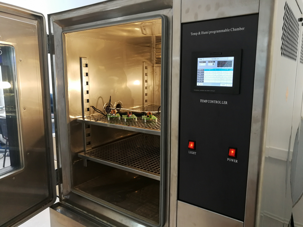
Environmental Stress Testing
Environmental stress testing subjects the PCB to extreme conditions like temperature cycling or vibration to assess signal layer reliability. These tests help determine if thermal expansion or mechanical stress causes delamination or cracks that could disrupt signal paths. Standards such as IPC-6012E provide guidelines for acceptable performance under such conditions, ensuring long-term durability.
Best Practices for Signal Layer Design and Testing
Achieving optimal signal layer performance requires careful design and rigorous testing. Below are actionable best practices for electrical engineers to follow during the development process.
- Optimize Layer Stackup: Arrange signal layers between ground planes to reduce electromagnetic interference. A well-planned stackup minimizes crosstalk and ensures stable impedance.
- Control Trace Geometry: Maintain consistent trace width and spacing to achieve uniform impedance. Use simulation tools to predict and adjust for potential mismatches.
- Incorporate Test Points: Include accessible test points in the design for easy signal integrity testing and impedance verification during prototyping.
- Adhere to Standards: Follow guidelines from standards like IPC-A-600K for acceptability criteria of printed boards. This ensures designs meet industry benchmarks for quality.
- Validate with Prototypes: Test early prototypes using TDR testing and other methods to identify and resolve signal layer issues before full-scale production.
Troubleshooting Common Signal Layer Issues
Even with meticulous design, signal layer issues can arise due to manufacturing variances or unforeseen design flaws. Understanding how to troubleshoot these problems is crucial for engineers.
One common issue is crosstalk, where signals on adjacent traces interfere with each other. This can often be mitigated by increasing trace spacing or adding shielding layers. Another frequent problem is signal reflection due to impedance mismatches, which can be identified through TDR testing and corrected by adjusting trace dimensions or termination strategies. Additionally, noise from power planes can couple into signal layers, necessitating careful placement of decoupling capacitors near critical components. By systematically addressing these issues with targeted PCB testing methods, engineers can ensure robust performance.
Conclusion
Signal layers play a pivotal role in the performance of printed circuit boards, particularly in high-speed and high-frequency applications. Through comprehensive signal layer testing, including signal integrity testing, impedance testing, and TDR testing, engineers can validate design performance and prevent costly failures. By adhering to established industry standards and implementing best practices, such as optimized layer stackups and thorough prototype validation, reliable signal transmission becomes achievable. As electronic systems grow more complex, the importance of rigorous PCB testing methods only increases, ensuring that designs meet the demands of modern technology with precision and durability.
FAQs
Q1: What is signal layer testing and why is it important for PCB design?
A1: Signal layer testing evaluates how well electrical signals travel through a PCB's dedicated layers without distortion. It is crucial for identifying issues like crosstalk or impedance mismatches that can degrade performance. For high-speed designs, ensuring signal integrity through testing prevents data errors and system failures, maintaining reliability in critical applications.
Q2: How does impedance testing contribute to signal integrity in PCBs?
A2: Impedance testing verifies that signal paths maintain consistent opposition to current flow, preventing reflections that cause signal loss. By ensuring traces match the specified impedance, engineers can minimize distortions. This process is vital for high-frequency designs where even small mismatches can significantly impact signal integrity and overall performance.
Q3: What role does TDR testing play in PCB validation?
A3: Time-Domain Reflectometry (TDR) testing detects discontinuities or faults in signal paths by analyzing reflected pulses. It helps locate impedance mismatches or breaks in traces, especially in multilayer boards. TDR testing is essential for diagnosing issues early, allowing engineers to refine designs before production and ensure reliable signal transmission.
Q4: Which PCB testing methods are most effective for signal layer issues?
A4: Effective PCB testing methods for signal layers include signal integrity testing for signal quality, impedance testing for trace consistency, and TDR testing for fault detection. Additionally, functional testing under real conditions and environmental stress testing per standards like IPC-6012E ensure long-term reliability, addressing both design and manufacturing flaws comprehensively.
References
IPC-6012E — Qualification and Performance Specification for Rigid Printed Boards. IPC, 2020.
IPC-A-600K — Acceptability of Printed Boards. IPC, 2020.