Introduction
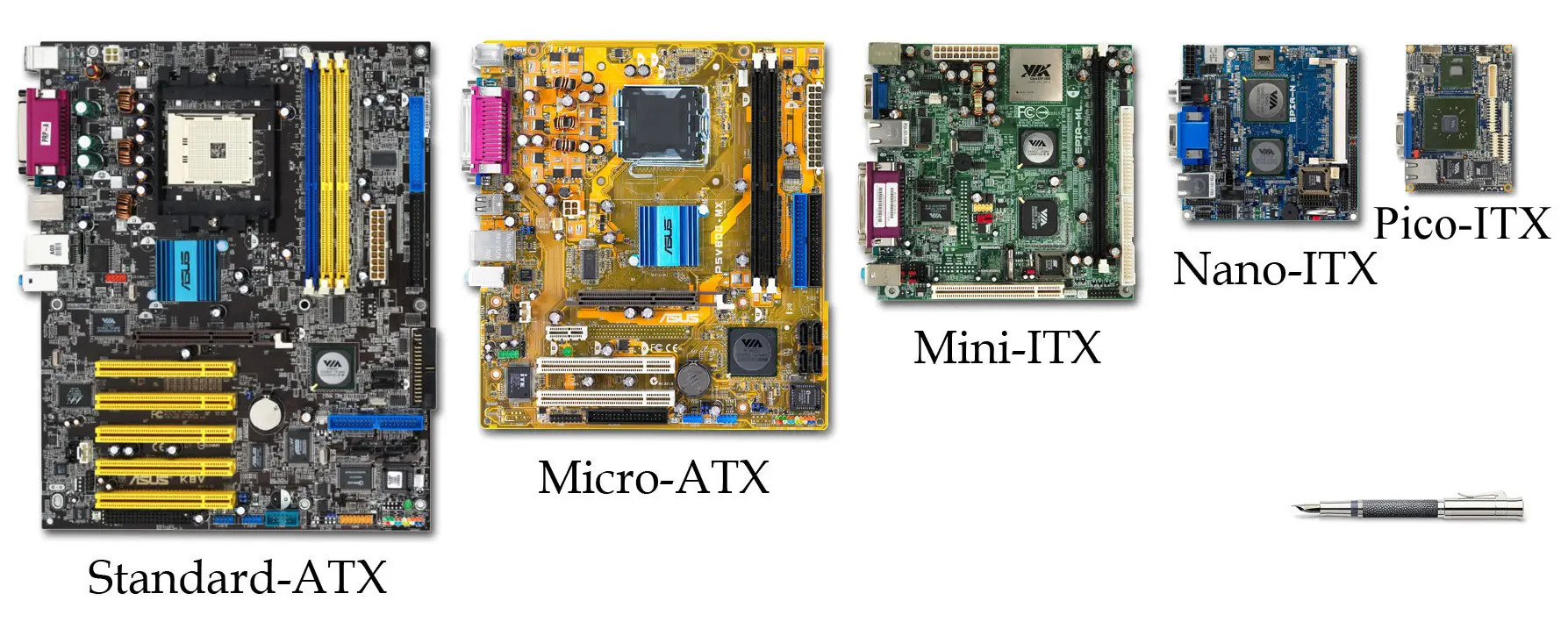
In PCB design, the form factor, defined by board dimensions, shape, and overall thickness profile, plays a critical role in determining the optimal PCB layer stack-up. Engineers must balance routing density, mechanical stability, and electrical performance when selecting layer counts and arrangements. A mismatched stack-up can lead to issues like signal degradation or manufacturing defects, while a well-planned one enhances reliability. This article explores how form factor constraints guide multilayer PCB design choices, focusing on impedance control and signal integrity. By understanding these relationships, designers can achieve superior performance tailored to specific applications. Key considerations include board size influencing layer symmetry and thickness dictating dielectric spacing.
What Is PCB Layer Stack-Up and Why Does Form Factor Matter?
PCB layer stack-up refers to the precise arrangement of conductive copper layers, insulating dielectrics, and power or ground planes in a multilayer board. Each layer serves a purpose, such as signal routing, power distribution, or reference planes for controlled impedance. Form factor directly influences this stack-up because larger boards experience greater thermal expansion stresses, necessitating symmetric constructions to minimize warpage. Smaller, compact form factors allow for higher layer counts in denser designs but require tighter control over via aspect ratios. In high-frequency applications, the stack-up must support signal integrity stack-up strategies to prevent crosstalk and reflections. Ultimately, aligning stack-up with form factor ensures manufacturability and performance meet design goals.
The relevance stems from real-world constraints in electric engineering projects. For instance, consumer electronics favor slim profiles, pushing for thin multilayer PCB designs with optimized layer pairing. Industrial controls often use larger panels where mechanical robustness overrides density. Poor form factor-stack-up matching can amplify electromagnetic interference or compromise PCB impedance control. Standards like IPC-2221 provide foundational guidelines for these decisions, emphasizing balanced layer distribution.
Technical Principles: How Form Factor Shapes Layer Selection
Form factor parameters, particularly board length and width, dictate the number of layers needed for routing complexity. Wider boards accommodate more parallel traces, potentially requiring additional signal layers, while elongated shapes demand careful plane placement to maintain uniform fields. Thickness profile further constrains options, as thinner boards limit core and prepreg thicknesses, affecting dielectric constants in the stack-up. Asymmetric stack-ups on large form factors lead to bow and twist during lamination, compromising flatness. Engineers evaluate these factors early to select layer counts that support both density and stability.
In multilayer PCB design, signal integrity stack-up relies on proximity between signal layers and adjacent reference planes. Form factor influences this by setting boundaries on total board height, which determines feasible dielectric thicknesses for impedance matching. High aspect ratio boards, common in compact enclosures, heighten via reliability concerns, favoring fewer layers with blind or buried vias. Thermal management also ties in, as larger surfaces dissipate heat differently, requiring power planes positioned according to form factor. These principles ensure the stack-up aligns with the physical constraints of the design.
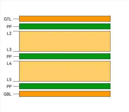
For high-frequency PCB stack-up, form factor amplifies challenges in wave propagation. Narrow, high-density boards need stripline configurations where signals are embedded between planes, controlled by dielectric spacing dictated by overall thickness. Broad panels benefit from microstrip layouts on outer layers for easier probing, but demand extensive ground flooding to contain fields. Impedance variations arise from form factor-induced manufacturing tolerances, such as panel bowing affecting etch uniformity. Proper layer sequencing mitigates these, preserving characteristic impedance across the board.
Mechanisms Behind Performance Impacts
Electrical performance hinges on how form factor interacts with stack-up electromagnetics. In PCB impedance control, trace width, spacing, and surrounding dielectric thicknesses define transmission line characteristics, all scaled to board dimensions. Larger form factors introduce longer trace runs prone to losses, necessitating more ground layers for return paths. Signal reflections intensify in mismatched environments, where form factor limits plane coverage. Multilayer arrangements with interleaved planes reduce loop inductance, crucial for compact designs.
Mechanically, form factor governs warpage susceptibility per IPC-6012 qualification criteria. Thick stacks on thin boards create imbalance, exacerbating CTE mismatches during reflow. Symmetric pairings, like signal-plane-signal, distribute stresses evenly, vital for rectangular or irregular shapes. High layer counts amplify these effects on oversized panels, requiring core balancing. Vibration-prone applications further demand robust stack-ups matched to form factor.
Thermally, power distribution layers must align with form factor heat flow paths. Dense, small boards concentrate hotspots, benefiting from embedded planes near components. Expansive designs spread dissipation, allowing outer-layer planes. Stack-up choices thus optimize via thermal resistance without specific metrics.
Best Practices for Multilayer PCB Design Aligned with Form Factor
Start with form factor analysis to estimate layer needs: compact boards suit 4-8 layers for density, while expansive ones prioritize 6-12 for integrity. Employ symmetric stack-ups universally, mirroring top and bottom halves to counter warpage. Pair high-speed signals with immediate ground planes for capacitance coupling, enhancing signal integrity stack-up. For high-frequency PCB stack-up, prioritize inner layers for sensitive nets, reserving surfaces for low-speed or shielding.
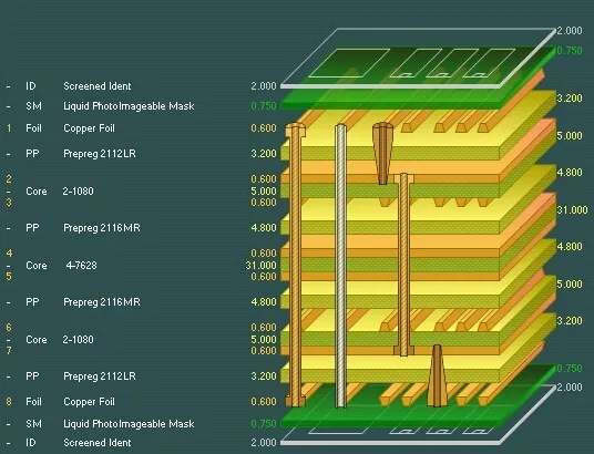
Control impedance through consistent dielectric stacks, adjusting for total thickness. Use plane splits judiciously, ensuring stitching vias bridge gaps per design rules. Simulate stack-up early, factoring board outline for edge effects. Validate with coupon structures on panels matching form factor. These practices, rooted in IPC-2141 for impedance, streamline multilayer PCB design.
Fabrication considerations include aspect ratios scaled to board size; avoid excessive depths in small form factors. Select prepregs for uniform flow, preventing voids in dense layers. Test stack-up prototypes under thermal cycling to confirm form factor compatibility.
Case Study Insights: Optimizing for Diverse Form Factors
Consider a mid-sized control board versus a compact RF module. The control board, with broader dimensions, adopted an 8-layer symmetric stack-up with dual ground planes for EMI containment. This addressed routing density while maintaining flatness. The RF module, constrained by slim profile, used a 6-layer high-frequency PCB stack-up with tight signal-plane coupling for phase stability. Both leveraged form factor to refine PCB layer stack-up, yielding reliable performance.
Troubleshooting common pitfalls involves auditing stack-up against outline. Excessive layers on thin boards cause delamination; remedy with hybrid cores. Large panels with asymmetric builds show bow; symmetrize immediately.
Conclusion
PCB form factor profoundly shapes layer selection and stack-up configuration, directly impacting impedance control, signal integrity, and mechanical reliability. Engineers achieve optimal multilayer PCB design by prioritizing symmetry, plane proximity, and thickness alignment. High-frequency applications demand specialized stack-ups tailored to dimensional constraints. Adhering to standards ensures consistency across projects. Thoughtful integration elevates performance, reducing iterations and costs.
FAQs
Q1: How does board size affect PCB layer stack-up choices?
A1: Larger boards require more robust PCB layer stack-up with additional ground planes to manage EMI and maintain signal integrity stack-up over longer traces. Symmetric arrangements prevent warpage from thermal stresses. Compact sizes favor denser layers but demand precise via control. Always align layer count with routing needs for efficiency.
Q2: What role does thickness play in multilayer PCB design?
A2: Thickness dictates dielectric spacing in multilayer PCB design, influencing PCB impedance control and layer feasibility. Thinner profiles limit high layer counts due to aspect ratio constraints. High-frequency PCB stack-up benefits from controlled heights for striplines. Balance with mechanical stability for overall performance.
Q3: Why prioritize symmetric stack-ups for signal integrity?
A3: Symmetric stack-ups enhance signal integrity stack-up by equalizing expansion, reducing bow and twist. This is critical for PCB impedance control uniformity across form factors. Paired planes shield signals effectively. Follow guidelines for reliable high-speed operation.
Q4: Best practices for high-frequency PCB stack-up in compact form factors?
A4: Embed sensitive traces between planes in high-frequency PCB stack-up for coupling. Maintain consistent dielectrics for impedance matching. Use blind vias to save space. Symmetric builds ensure flatness despite density. Simulate for crosstalk minimization.
References
IPC-2221 — Generic Standard on Printed Board Design. IPC
IPC-2141 — Design Guide for High-Speed Controlled Impedance Circuit Boards. IPC
IPC-6012E — Qualification and Performance Specification for Rigid Printed Boards. IPC, 2015


