Introduction
Power supply circuits form the backbone of any electronic project, providing stable voltage to sensitive components. For electronic hobbyists, transitioning from breadboard prototypes to custom printed circuit boards (PCBs) unlocks reliability and compactness. KiCad stands out as a free, open-source tool suite perfect for this task, offering schematic capture and PCB layout capabilities without licensing costs. This KiCad PCB design tutorial walks you through creating a power supply PCB from concept to completion, focusing on a simple regulated design suitable for hobby projects like LED drivers or microcontroller supplies. By following these steps, you will learn to build a KiCad power supply PCB that handles input voltages efficiently while minimizing noise and heat. Expect to cover schematic entry, footprint assignment, routing, and verification, all tailored for beginners advancing their skills.
Why Power Supply PCBs Matter for Electronic Hobbyists
A power supply PCB converts and regulates raw input power into usable output for circuits, far surpassing jumper-wire setups in performance. Hobbyists often face issues like voltage drops or ripple on breadboards, which custom PCBs eliminate through dedicated traces and planes. These boards support applications from 5V USB supplies to 12V motor drivers, enabling compact enclosures and repeatable results. Designing one in KiCad empowers you to iterate quickly, test real-world loads, and scale projects. Moreover, professional layouts reduce electromagnetic interference (EMI), crucial for analog sensors or audio amps. Understanding this foundation ensures your KiCad power supply PCB integrates seamlessly with other modules.
Key Technical Principles of Power Supply Design
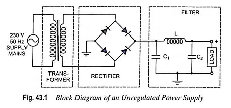
Power supplies rely on regulation to maintain output voltage despite load or input variations, using linear or switching topologies. Linear regulators dissipate excess power as heat, suiting low-current needs, while switching types like buck converters offer efficiency for higher loads. Key mechanisms include input filtering to block transients, output decoupling for stability, and protection diodes against reverse polarity. Heat management prevents component failure, with thermal vias and pads distributing dissipation. Conductor sizing follows guidelines in IPC-2221C to handle current without excessive voltage drop or overheating. Grounding strategies, such as star or plane configurations, minimize noise loops essential for clean power delivery.
Step 1: Setting Up Your KiCad Project for Power Supply Design
Launch KiCad and create a new project by selecting File > New > Project, naming it something like "PowerSupplyBoard". This generates folders for schematics, PCBs, and libraries. Open the Schematic Editor (Eeschema) to begin circuit capture. Add hierarchical sheets if your design grows complex, but start flat for simplicity. Set global labels for power nets like VIN and VOUT early. Save frequently to maintain project integrity across tools.
Step 2: Creating the Power Supply PCB Schematic in KiCad
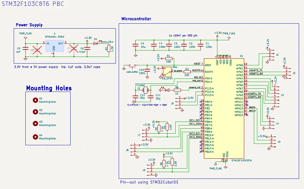
In Eeschema, place symbols from the library browser: search for a generic voltage regulator IC, electrolytic capacitors for input and output, and a diode. Connect them logically: input to regulator IN pin via capacitor, output from OUT pin with capacitor to ground, diode across input for protection. Add power flags (PWR_FLAG) on VCC and GND nets to define global power. Use labels for nets like "5V_OUT" to clarify connections. Annotate components via Tools > Annotate Schematic, ensuring unique references. Run Electrical Rules Check (ERC) under Inspect > Electrical Rules Checker to catch unconnected pins or missing flags. This power supply PCB schematic KiCad process verifies logic before layout.
Step 3: Assigning Footprints to Your Schematic Symbols
With the schematic complete, double-click symbols to assign footprints: select from the Footprint Library, matching package types like TO-220 for regulators or 1206 for SMD caps. KiCad's libraries follow conventions aligned with IPC-7351 for surface mount land patterns, ensuring reliable soldering. For through-hole parts, verify lead spacing. Use the Footprint Assignment Tool (Tools > Assign Footprints) for batch editing. Update the schematic view to confirm assignments. This step bridges schematic to physical board, preventing layout mismatches.
Step 4: Generating Netlist and Starting PCB Layout
Export the netlist via Tools > Generate Netlist, saving it to link schematic changes. Switch to PCB Editor (Pcbnew), where the netlist import places components as a rat's nest of airwires. Set board outline: Draw > Edge.Cuts, sketching a rectangle or custom shape, typically 50mm x 50mm for prototypes. Adjust design rules under Setup > Design Rules: set min trace width to 0.25mm, clearance 0.2mm, via sizes appropriately. Place components intuitively: regulators near edges for heatsinks, caps close to IC pins. Lock positions after arrangement to avoid shifts during routing.
Step 5: Routing the Power Supply PCB Layout in KiCad
Prioritize power traces: use the interactive router (Route > Interactive Router) for thick high-current paths from input to regulator. Widen traces via Properties panel, consulting IPC-2221C charts for ampacity based on copper thickness. Fill zones for ground: Zone > Add Filled Zone on bottom layer, naming it GND, pouring copper for low impedance return paths. Route signal nets last, avoiding sharp angles over 45 degrees. Add vias for multilayer if needed, but single or double-layer suits hobby power supplies. Run Design Rule Check (DRC) under Inspect > Design Rules Checker to flag violations like insufficient clearance.
Step 6: Adding Finishing Touches and Verification
Place silkscreen labels for polarity and values using the text tool. Add mounting holes via Place > Footprint > select hole library. Generate 3D view (View > 3D Viewer) to inspect mechanically. Plot Gerber files under File > Plot, selecting layers like F.Cu, B.Cu, Edge.Cuts, F.Silkscreen. Export drill files and check with a viewer. Final DRC and ERC confirm compliance, aligning with IPC-6012F performance specs for rigid boards. This completes your KiCad power supply PCB ready for fabrication.
Best Practices and Troubleshooting for Power Supply PCBs
Orient electrolytic caps for easy assembly, and place high-current paths away from signals to cut EMI. Use stitching vias around ground zones for better equipotential. For heat, add thermal reliefs on pads and consider copper pours under regulators. Common pitfalls include forgetting power flags causing ERC errors, or undersized traces leading to drops; always iterate DRC early. If ripple appears post-build, add more decoupling or ferrite beads. These practices ensure robust operation matching industry benchmarks.
Conclusion
Designing a power supply PCB in KiCad transforms hobby projects into professional-grade hardware. From schematic capture to routed layout, each step builds skills in regulation, routing, and verification. Key takeaways include prioritizing power integrity, leveraging standards like IPC-2221C for traces, and using DRC religiously. Hobbyists gain confidence tackling complex boards, paving the way for integrated systems. Start simple, prototype often, and refine based on tests. Your KiCad power supply PCB will power endless innovations reliably.
FAQs
Q1: How do I begin a KiCad power supply PCB project?
A1: Open KiCad, create a new project, and launch Eeschema for schematic design. Add symbols for regulator, capacitors, and diode, connecting with wires and power flags. Annotate and run ERC before footprint assignment. Import netlist to Pcbnew for layout. This structured start ensures smooth KiCad PCB design tutorial flow, avoiding common setup errors.
Q2: What are essential checks in power supply PCB schematic KiCad?
A2: Verify connections with ERC, focusing on unconnected pins and power flags. Annotate for unique references and assign IPC-7351 compliant footprints. Label nets clearly for traceability. Test netlist generation to confirm schematic-to-PCB sync. These steps prevent layout issues in your power supply PCB schematic KiCad.
Q3: How to route high-current traces in power supply PCB layout KiCad?
A3: Use wide traces per IPC-2221C guidelines, routing input and output first. Add ground planes for returns and thermal vias under hot components. Maintain clearances and run DRC. Pour zones and stitch with vias. This optimizes power supply PCB layout KiCad for efficiency and reliability.
Q4: Why use design rules in KiCad power supply PCB design?
A4: Design rules enforce min widths, clearances, and via sizes, catching errors early. Customize for power needs like thicker traces. Align with IPC-6012F for quality. DRC flags violations pre-fabrication. Essential for hobbyists achieving professional KiCad power supply PCB results.
References
IPC-2221C — Generic Standard on Printed Board Design. IPC, 2023
IPC-7351 — Generic Requirements for Surface Mount Design and Land Pattern Standard. IPC, 2005
IPC-6012F — Qualification and Performance Specification for Rigid Printed Boards. IPC, 2023


