Introduction
Prototyping a navigation system PCB opens up exciting possibilities for electronic hobbyists working on projects like drone flight controllers, robotic rovers, or portable GPS trackers. These custom boards integrate sensors, receivers, and processors to determine position, direction, and speed in real-world applications. For hobbyists, the prototyping process combines creativity with practical engineering, allowing you to test ideas quickly without committing to large production runs. Navigation PCB prototyping services make this accessible by offering fast turnaround times and reliable results tailored to small batches. Whether you are building a handheld navigator for hiking or an autonomous boat controller, a well-prototyped PCB ensures your system performs accurately under various conditions. This guide walks you through each step, from initial design to final testing, helping you avoid common pitfalls and achieve professional-grade outcomes.
What Is a Navigation System PCB and Why Does It Matter for Hobbyists?
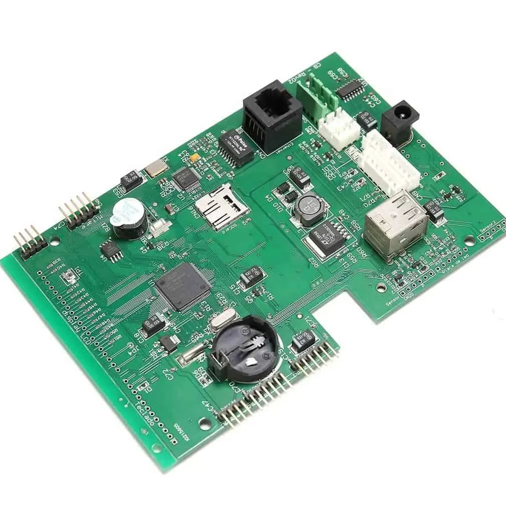
A navigation system PCB serves as the central hub for components that enable location tracking and orientation sensing, such as GNSS receivers, inertial measurement units (IMUs), and magnetometers. These boards process signals from satellites or onboard sensors to compute real-time position data, which is crucial for applications ranging from hobby drones to wearable fitness devices. In the hobbyist space, navigation PCBs stand out because they demand a balance of compact size, low power consumption, and resistance to environmental factors like vibration and temperature swings. Prototyping such boards matters because off-the-shelf modules often lack customization for specific project needs, such as integrating unique sensor fusions or minimizing weight for aerial vehicles.
The relevance grows with the rise of DIY automation projects, where precise navigation can make or break functionality. For instance, a poorly prototyped board might suffer from signal interference, leading to erratic positioning in your robot. By focusing on navigation PCB quick-turn PCB options, hobbyists can iterate designs rapidly, testing prototypes in days rather than weeks. This approach not only saves time but also builds confidence in scaling up to more complex systems. Ultimately, mastering navigation PCB prototyping empowers you to create reliable, innovative gadgets that perform in dynamic environments.
Key Technical Principles for Navigation System PCBs
Navigation system PCBs rely on several core engineering principles to handle high-frequency signals and sensitive analog components effectively. GNSS signals operate at specific frequencies, requiring controlled impedance traces to prevent signal loss or distortion during transmission from antennas to receivers. Ground planes play a vital role in shielding sensitive traces from electromagnetic interference, which is common in environments with motors or power supplies. Layer stackup decisions influence thermal dissipation and mechanical stability, especially for boards exposed to movement or outdoor conditions. Power distribution networks must deliver clean, stable voltages to sensors and microcontrollers, often using decoupling capacitors placed close to IC pins.
Another critical aspect is component placement strategy, which minimizes trace lengths for high-speed signals while separating analog and digital sections to reduce crosstalk. For hobbyists, understanding these principles means prioritizing RF performance without needing advanced simulation tools initially. Mechanical considerations, such as via placement and solder mask coverage, ensure durability during handling or enclosure mounting. Adhering to standards like IPC-6012E for rigid board qualification helps maintain consistency in fabrication quality. These foundational mechanisms form the backbone of a robust prototype, setting the stage for reliable navigation performance.
Step-by-Step Guide to Prototyping Your Navigation System PCB
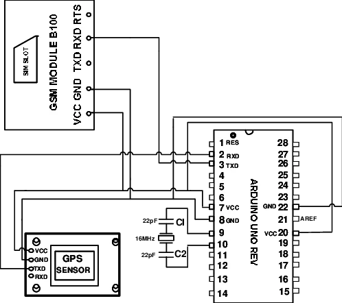
Step 1: Define Requirements and Create the Schematic
Start by outlining your project's needs, including size constraints, power budget, and accuracy targets for positioning. List essential components like a GNSS module, microcontroller, IMU, and power regulators, ensuring compatibility in terms of voltage and interfaces. Draw the schematic by connecting these elements logically, with attention to power rails and signal paths. Add pull-up resistors, bypass capacitors, and protection diodes where necessary to handle noise or ESD events. For hobbyists, keep the design simple initially, focusing on core navigation functions before adding extras like displays or wireless modules. Verify the schematic through a design rule check to catch errors early.
Step 2: PCB Layout and File Generation
Transition to layout by importing the schematic and placing components strategically, with RF sections isolated from noisy digital areas. Route traces with appropriate widths for current carrying and impedance control, using ground pours to fill unused spaces. Define the board outline, drill holes for mounting, and specify silkscreen labels for easy assembly. Generate output files including Gerbers for layers, drill files, Bill of Materials (BOM), and pick-and-place data for assembly. Hobbyists benefit from navigation PCB PCB fabrication processes that support small quantities and standard lead times. Double-check layer alignment and annotation to avoid costly reprints.
Step 3: Select Navigation PCB Quick-Turn PCB Fabrication
Choose fabrication parameters suited to your design, such as 2- or 4-layer boards with FR-4 material for cost-effectiveness in prototypes. Specify copper thickness, solder mask color, and surface finish like HASL or ENIG for better solderability. Quick-turn options typically deliver panels in 24 to 72 hours, ideal for iterative hobby projects. Upload Gerbers and review the fabricator's DFM report for issues like minimum trace spacing or annular ring violations. Fabrication follows controlled processes to ensure planarity and trace integrity, critical for navigation signal fidelity. Once received, inspect visually for defects before proceeding.
Step 4: Navigation PCB PCB Assembly
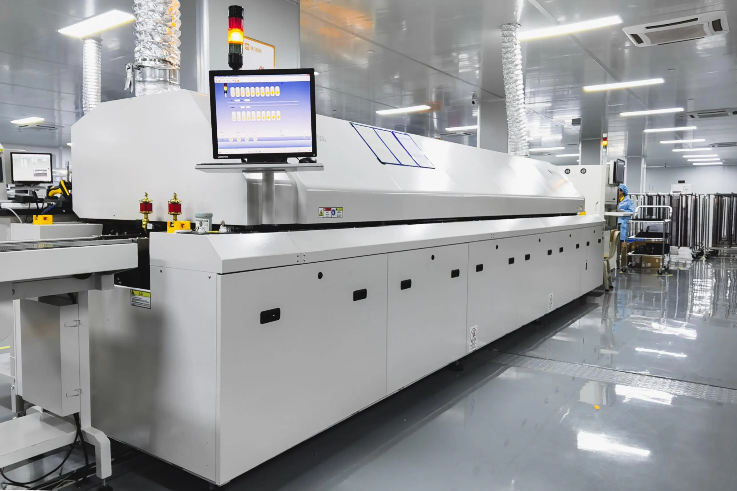
Prepare for assembly by printing a stencil if using reflow soldering, or opt for hand-soldering for low volumes. Place components according to the pick-and-place file, starting with smallest passives and progressing to larger ICs. Reflow the board in an oven profile compliant with component specifications, monitoring peak temperatures to avoid damage. For hobbyists, hybrid assembly combining machine placement with manual work suits navigation PCB PCB assembly needs. Clean flux residues post-assembly and apply conformal coating if environmental protection is required. Perform initial continuity checks with a multimeter to confirm connections.
Step 5: Comprehensive Navigation PCB Testing
Testing begins with power-up verification, ensuring no shorts and stable voltages across rails. Functional tests involve connecting to a GNSS antenna and verifying satellite lock under open-sky conditions, alongside IMU calibration for accurate orientation. Use oscilloscopes to probe signals for noise levels and logic analyzers for communication protocols like UART or I2C. Environmental testing simulates real-world stresses, such as vibration on a shaker table or thermal cycling. Navigation PCB testing protocols reveal issues like poor ground returns causing position drift. Iterate by revising the design if failures occur, leveraging quick-turn cycles for fixes.
Adherence to IPC-A-600K acceptability criteria during inspection ensures defects do not propagate. Document results in a test report for future reference.
Troubleshooting Common Issues in Navigation PCB Prototypes
Hobbyists often encounter GPS signal dropouts due to inadequate ground shielding or trace routing near high-current paths. Mitigate this by rerouting signals away from power planes and adding shielding cans over receivers. Another frequent problem is IMU drift from vibration, addressed by mounting sensors on damped substrates or using mechanical isolation. Power supply ripple can corrupt analog readings, so incorporate LC filters and verify with spectrum analysis. If assembly yields cold joints, refine reflow profiles or stencil apertures. Systematic troubleshooting, combined with J-STD-001 soldering standards, resolves most issues efficiently.
Conclusion
Prototyping a navigation system PCB equips electronic hobbyists with the tools to bring location-aware projects to life, from autonomous vehicles to tracking devices. By following this step-by-step process, you streamline design, fabrication, assembly, and testing while integrating keywords like navigation PCB prototyping services for targeted searches. Key takeaways include prioritizing signal integrity, leveraging quick-turn options, and applying basic standards for quality. With practice, your prototypes will evolve into reliable systems ready for field deployment. Experiment iteratively, document learnings, and enjoy the satisfaction of a functional custom board.
FAQs
Q1: What are navigation PCB prototyping services, and how do they benefit hobbyists?
A1: Navigation PCB prototyping services provide end-to-end support from design files to assembled boards, specializing in small runs with fast delivery. Hobbyists gain access to professional fabrication and assembly without large minimum orders, enabling quick iterations for projects like drone navigation. These services handle DFM checks and basic testing, reducing errors and turnaround to days.
Q2: How long does navigation PCB quick-turn PCB fabrication typically take?
A2: Navigation PCB quick-turn PCB fabrication usually completes in 24 to 72 hours for standard 2-layer boards, depending on complexity and queue. This speed suits hobbyists needing rapid prototypes for testing GNSS integration or sensor fusion. Always confirm with panel size and shipping options for total timeline.
Q3: What steps are involved in navigation PCB PCB assembly for prototypes?
A3: Navigation PCB PCB assembly starts with stencil printing for solder paste, followed by component placement and reflow soldering. Hobbyists can hand-assemble simpler boards or use services for precision. Post-process cleaning and inspection ensure reliability before functional navigation PCB testing.
Q4: Why is navigation PCB testing essential in prototyping?
A4: Navigation PCB testing validates signal acquisition, power stability, and environmental resilience, catching issues like interference early. For hobbyists, it confirms position accuracy in real scenarios, preventing project failures. Basic bench tests evolve to field trials for comprehensive assurance.
References
IPC-6012E — Qualification and Performance Specification for Rigid Printed Boards. IPC, 2017
IPC-A-600K — Acceptability of Printed Boards. IPC, 2020
J-STD-001G — Requirements for Soldered Electrical and Electronic Assemblies. IPC, 2011


