Introduction
Test and measurement printed circuit boards (PCBs) serve as the backbone for validating electronic designs, ensuring signals, voltages, and power delivery meet precise specifications in laboratory and production environments. These specialized boards handle high-frequency signals, sensitive analog measurements, and stable power distribution, where even minor imperfections can lead to significant errors. Engineers rely on them for oscilloscope probes, data acquisition systems, and calibration fixtures, making reliability paramount. Optimizing PCB performance involves targeted testing to identify issues like signal distortion, inaccurate voltage readings, and power fluctuations early in the design cycle. By minimizing PCB errors through systematic techniques, teams can achieve higher accuracy, reduce rework, and accelerate time-to-market. This article explores proven methods for PCB testing for signal distortion, PCB testing for inaccurate voltage, and PCB testing for power issues, drawing on engineering principles to guide electric engineers.
Understanding Test and Measurement PCBs and Their Critical Role
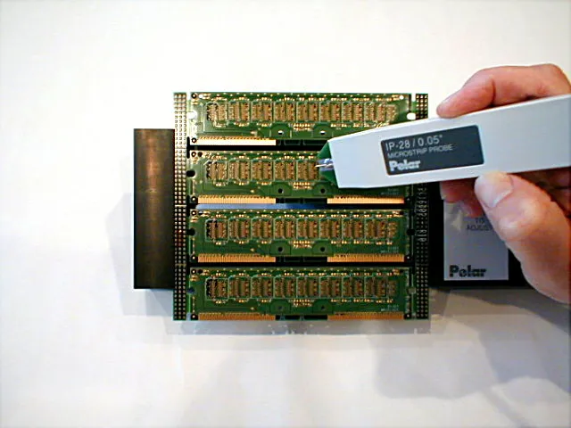
Test and measurement PCBs differ from standard boards by prioritizing low noise, controlled impedance, and minimal parasitics to faithfully reproduce signals without alteration. They incorporate features like matched transmission lines, dedicated ground planes, and precision vias to support applications from RF characterization to power analyzer interfaces. In high-stakes fields like telecommunications and aerospace, these boards ensure measurements reflect true device behavior rather than board-induced artifacts. Poor performance here amplifies errors downstream, compromising design validation and certification processes. Engineers must grasp how material properties, layer stackup, and routing choices directly impact measurement fidelity. Adhering to guidelines in IPC-2141 for controlled impedance helps maintain signal integrity across frequencies.
The relevance intensifies with rising data rates and precision demands, where test PCBs act as intermediaries between devices under test and instruments. Subtle deviations, such as trace length mismatches or via stubs, propagate into distorted waveforms or offset readings. Optimizing PCB performance starts with recognizing these interactions during the design phase. Proactive PCB testing for signal distortion, voltage accuracy, and power stability prevents cascading failures. Ultimately, robust test PCBs enable confident scaling from prototype to production.
Key Sources of Errors in Test and Measurement PCBs
Errors in test and measurement PCBs often stem from signal propagation challenges, where reflections and crosstalk degrade waveform quality. Signal distortion arises from impedance discontinuities at vias, bends, or connectors, causing overshoot, ringing, or attenuation. Inaccurate voltage measurements frequently result from ground bounce, probe loading, or insufficient decoupling, leading to offsets or noise injection. Power issues manifest as voltage droops under load or ripple from inadequate plane distribution, affecting measurement baselines. These problems compound in multilayer boards, where coupling between layers exacerbates issues. Understanding root causes allows engineers to apply targeted PCB testing techniques.
Material selection plays a pivotal role, as dielectrics with high loss tangent introduce phase shifts and amplitude loss at gigahertz frequencies. Layout asymmetries, like uneven trace spacing, promote crosstalk, coupling unwanted energy between channels. Thermal expansion mismatches during operation can warp boards, altering contact integrity and introducing intermittent errors. Environmental factors, such as EMI from nearby sources, further degrade performance. Systematic analysis reveals these patterns, guiding refinements.
PCB Testing Techniques for Signal Distortion
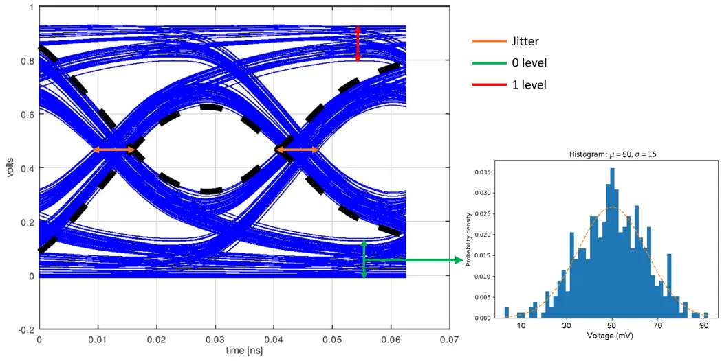
PCB testing for signal distortion begins with Time Domain Reflectometry (TDR), which launches a step signal to detect impedance variations along traces. Discontinuities appear as reflections, pinpointing locations for correction like via optimization or stub removal. Engineers sweep frequencies with a Vector Network Analyzer (VNA) to measure S-parameters, quantifying insertion loss and return loss. Eye diagram analysis overlays multiple bit transitions, revealing jitter, closure, and height degradation indicative of distortion. These methods quantify issues before assembly, enabling layout iterations. Calibration with open-short-load standards ensures measurement accuracy.
Crosstalk testing involves injecting signals on aggressor lines while monitoring victims for induced noise, using near-end and far-end coupling metrics. Frequency-domain sweeps isolate resonances from coupled structures. De-embedding techniques account for test fixture parasitics, yielding true channel responses. Combining TDR with oscilloscope captures provides time and frequency insights. Regular verification against design targets minimizes PCB errors in high-speed applications. These techniques form the core of optimizing PCB performance for signal fidelity.
Strategies for PCB Testing for Inaccurate Voltage
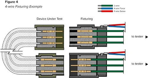
Inaccurate voltage in test PCBs often traces to poor ground referencing or capacitive probe effects, inflating or attenuating readings. Differential probing minimizes common-mode noise, preserving accuracy across dynamic ranges. Engineers perform Kelvin four-wire measurements to eliminate lead resistance drops, ideal for low-level sensing. Noise spectral analysis with FFT on oscilloscopes identifies 50/60 Hz pickup or switching harmonics. Decoupling capacitor placement testing under load simulates real conditions, spotting impedance peaks. These approaches directly address root causes.
Guard traces around sensitive nets shield from adjacent interference, verified through guarded Kelvin setups. Multi-point voltage mapping reveals gradients from IR drops in power planes. Temperature-controlled testing exposes thermal voltage coefficients in traces or connectors. Automated scripting on bench equipment accelerates parametric sweeps. By integrating these into the workflow, teams achieve sub-millivolt precision. PCB testing for inaccurate voltage thus becomes a repeatable process for reliability.
Tackling PCB Testing for Power Issues
Power integrity challenges in test PCBs include excessive ripple from decoupling shortfalls or plane splits causing current crowding. Impedance profiling via VNA on power distribution networks (PDN) maps resonances across frequencies. Transient response testing applies load steps, measuring droop and settling time with high-bandwidth scopes. DC IR drop analysis uses current injection to validate plane thickness adequacy. Ripple quantification under worst-case loads flags bypass capacitor efficacy. These tests ensure stable rails for accurate measurements.
Thermal imaging during power stress reveals hotspots from via current limits or plane voids. Bulk capacitance distribution optimization reduces low-frequency bounce. Simulation correlation with hardware validates PDN models pre-build. Iterative fixture redesign incorporates wider planes or embedded caps. PCB testing for power issues prevents measurement drift in long-duration tests. Mastering these yields robust power delivery.
Best Practices for Optimizing PCB Performance and Minimizing Errors
Optimizing PCB performance demands symmetric routing with length-matched pairs to avert skew in differential signals. Full ground planes beneath signal layers provide return paths, minimizing loop inductance. Via-in-pad or blind vias reduce stubs, preserving high-frequency response. Material choices with low dissipation factor curb attenuation, balanced against cost. Stackup planning allocates layers for power/ground interleaving, enhancing decoupling density. These layout tenets form the foundation.
Design for testability includes test points on every net, accessible without desoldering. Controlled impedance per IPC-TM-650 procedures ensures reproducibility across batches. Fabrication reviews catch drill breakout risks or plating voids early. Post-assembly burn-in stresses boards, exposing infant mortalities. Documentation of test limits facilitates yield analysis. By embedding these practices, engineers minimize PCB errors systematically.
Shielding enclosures or partitioned grounds isolate channels, verified through radiated susceptibility tests. Firmware-configurable attenuators adapt to signal amplitudes. Multi-stage filtering on power inputs suppresses noise. Peer reviews challenge assumptions, uncovering blind spots. Continuous metrics tracking refines processes over projects.
Troubleshooting Common Issues in Test PCBs
When signal distortion persists post-optimization, check for solder fillet capacitance at connectors using network analysis. Voltage inaccuracies may signal connector fretting; cycle mating tests confirm stability. Power droops under pulse loads point to ESL in ceramics; supplement with polymer caps. Warpage from CTE mismatch alters trace geometry; profilometry quantifies bow. Layer registration errors cause shorts; microsectioning verifies alignment. Logical deduction paired with IPC-TM-650 test methods resolves most anomalies.
Fixture resonance from mechanical modes couples mechanically to electrically; modal hammer testing identifies culprits. Probe grounding springs fatigue over cycles; replace with rigid Kelvin clips. Environmental chamber runs simulate field conditions, exposing latent weaknesses. Data logging correlates failures to variables like humidity. This structured troubleshooting minimizes PCB errors effectively.
Conclusion
Test and measurement PCBs demand meticulous attention to signal paths, voltage referencing, and power distribution to deliver trustworthy results. Techniques like TDR for distortion, Kelvin probing for voltage, and PDN profiling for power issues provide actionable insights. Integrating best practices such as controlled impedance, robust decoupling, and DFT ensures high performance. By prioritizing PCB testing for signal distortion, inaccurate voltage, and power issues, engineers minimize PCB errors while optimizing PCB performance. Consistent application yields reliable boards that accelerate innovation. Commit to these principles for superior outcomes.
FAQs
Q1: How can engineers perform effective PCB testing for signal distortion?
A1: PCB testing for signal distortion relies on TDR to detect impedance mismatches and eye diagram analysis to assess jitter and closure. VNAs measure S-parameters for loss and crosstalk quantification. Calibrate fixtures and de-embed parasitics for accuracy. These methods identify reflections from vias or bends early. Regular sweeps across operating frequencies ensure compliance, optimizing PCB performance in high-speed setups.
Q2: What steps address PCB testing for inaccurate voltage readings?
A2: Start with differential or Kelvin probing to avoid ground loops and lead drops during PCB testing for inaccurate voltage. Analyze noise spectra to isolate sources like EMI pickup. Verify decoupling under dynamic loads with scope transients. Guard traces enhance isolation. These techniques restore precision, minimizing PCB errors in sensitive analog chains.
Q3: What are key methods for PCB testing for power issues?
A3: For PCB testing for power issues, profile PDN impedance with VNAs and test transient droop via load steps. Quantify ripple under max current and map DC drops. Optimize planes and caps iteratively. Thermal scans spot hotspots. This approach stabilizes rails, supporting reliable measurements and optimizing PCB performance.
Q4: How to minimize PCB errors in test and measurement designs?
A4: Minimize PCB errors through symmetric routing, full ground planes, and IPC-TM-650 verified impedance control. Incorporate test points and shielding for accessibility. Stress test in chambers and correlate simulations. Peer reviews catch oversights. These practices yield low-noise, accurate boards for demanding applications.
References
IPC-2141 - Embedded Processes for Printed Boards with Controlled Impedance Characteristics. IPC.
IPC-TM-650 - Test Methods Manual. IPC.
IPC-6012E - Qualification and Performance Specification for Rigid Printed Boards. IPC, 2017


