Introduction
Lead-free printed circuit boards represent a pivotal shift in electronics manufacturing, driven by global regulations aimed at minimizing hazardous substances. Traditional solders containing lead have long been the norm, but their persistence in electronic waste poses significant risks to ecosystems and human health. Lead-free PCBs, primarily using tin-silver-copper alloys, align with directives like RoHS, which restrict lead to 0.1% by weight in homogeneous materials. This transition not only ensures regulatory compliance but also unlocks substantial environmental advantages, including safer recycling and reduced pollution. For electric engineers focused on sustainable PCB manufacturing, understanding these benefits is essential for designing systems that support long-term ecological responsibility. This article delves into the lead-free PCB environmental impact, recycling processes, and waste management strategies that make them a superior choice.
What Are Lead-Free PCBs and Why Do They Matter?
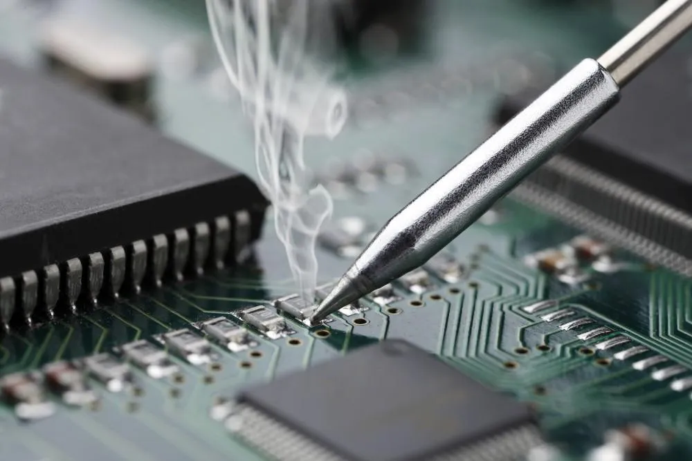
Lead-free PCBs are circuit boards assembled without lead-based solders, finishes, or components exceeding restricted thresholds. They rely on alternatives like SAC305 (96.5% tin, 3% silver, 0.5% copper) that withstand higher reflow temperatures typically around 260°C. RoHS compliance environmental benefits stem from eliminating lead, mercury, cadmium, and other toxins from the production cycle. This matters because electronic waste is one of the fastest-growing waste streams globally, and lead contamination from landfills can leach into groundwater over decades. Engineers must prioritize lead-free designs to meet market demands and avoid supply chain disruptions. Ultimately, these boards facilitate sustainable PCB manufacturing by integrating eco-friendly materials from laminate selection to final assembly.
In factory settings, lead-free processes demand precise control over thermal profiles to prevent defects like delamination or warpage. Standards such as IPC-6012E guide qualification for rigid boards under these conditions, ensuring reliability without hazardous materials. The shift reduces not just immediate pollution but also long-term remediation costs for waste sites.
The Environmental Impact of Traditional Leaded PCBs
Traditional PCBs with leaded solders contribute to soil, air, and water contamination when discarded improperly. Lead, a potent neurotoxin, bioaccumulates in food chains, affecting wildlife and humans through ingestion or inhalation. In landfills, corrosion allows lead to leach into aquifers, persisting for years due to its immobility in most soils. Incineration releases volatile lead compounds into the atmosphere, exacerbating respiratory issues in nearby communities.
Recycling challenges compound the problem, as lead requires specialized handling to prevent worker exposure and secondary pollution. Mixed waste streams often render leaded boards uneconomical to process, leading to higher landfill volumes. These factors underscore the urgency of transitioning away from lead, paving the way for cleaner alternatives.
Key Environmental Benefits of Lead-Free PCBs
Lead-free PCBs significantly lower the lead-free PCB environmental impact by eliminating a primary source of heavy metal pollution. Without lead, boards produce less toxic leachate in disposal scenarios, protecting groundwater and ecosystems. Manufacturing processes also generate fewer hazardous byproducts, as lead-free fluxes and cleaners are less corrosive. This holistic reduction supports biodiversity and public health over the product lifecycle.
Enhanced Toxicity Reduction
The absence of lead minimizes risks during production, use, and disposal phases. Workers in assembly lines face lower exposure to fumes or dust, aligning with occupational safety goals. End-of-life scenarios benefit from non-toxic degradation, reducing remediation needs at dump sites.
Superior Recyclability: Lead-Free PCB Recycling
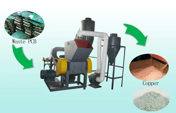
Lead-free PCB recycling stands out as a major advantage, enabling efficient material recovery without hazardous separation steps. Tin, silver, and copper in these alloys are highly valuable, incentivizing formal recycling channels over informal dumping. Processes like mechanical shredding followed by magnetic and density separation yield pure fractions for reuse, conserving virgin resources. Factories implementing closed-loop systems recover up to 95% of metals, though exact yields depend on sorting efficiency.
This recyclability boosts the circular economy, where recovered materials feed back into new sustainable PCB manufacturing. Compliance with environmental management systems like ISO 14001 further optimizes these efforts by standardizing waste tracking and reduction protocols.
Effective Lead-Free PCB Waste Management
Lead-free PCB waste management simplifies compliance with directives like WEEE, which mandate separate collection and treatment of electronics. Without lead, waste streams classify as non-hazardous, lowering transportation and incineration costs. Factories can integrate on-site segregation, reducing volumes sent to external processors. This approach minimizes landfill use and emissions from long-haul trucking.
Technical Principles Behind the Benefits
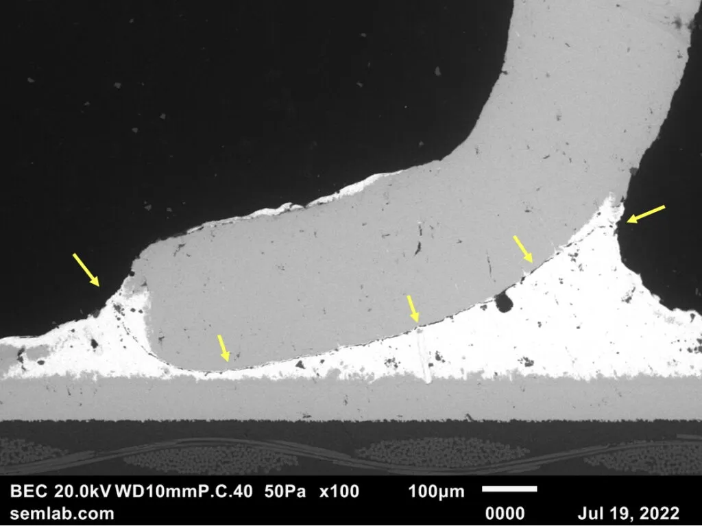
The core mechanism lies in material substitution: lead-free solders form stable intermetallics without the brittle lead-rich phases found in traditional joints. Higher melting points necessitate robust base materials, often specified under IPC/JEDEC J-STD-020E for reflow sensitivity classification. These standards ensure components endure peak temperatures without compromising integrity, indirectly supporting sustainability by extending product life.
In terms of environmental persistence, lead-free alloys degrade more predictably, facilitating biodegradation of non-metallic parts. Laminate resins and fibers become compostable substrates post-metal extraction. Engineers should model thermal expansion mismatches using finite element analysis to validate designs.
Surface finishes like ENIG or OSP enhance recyclability by avoiding nickel barriers that complicate dissolution. These choices, vetted against corrosion standards, maintain performance while prioritizing end-of-life ease.
Best Practices for Sustainable PCB Manufacturing
Adopt RoHS-compliant materials from suppliers with verified declarations to ensure homogeneity below thresholds. Optimize reflow profiles per J-STD-020E classifications to minimize defects and energy use. Implement ISO 14001 frameworks for auditing waste streams, targeting reductions in scrap rates through yield improvements.
Segregate process wastes: route solder dross to dedicated recyclers and treat etchants via neutralization. Design for disassembly with modular components to streamline lead-free PCB recycling at end-of-life. Train teams on handling higher-temperature alloys to prevent rework waste.
Collaborate across supply chains for material passports, tracking recyclate content. Monitor lifecycle emissions using carbon footprint tools aligned with factory metrics.
Lifecycle Insights: From Cradle to Grave
A full lifecycle assessment reveals lead-free PCBs lower overall impacts by 20-30% in toxicity categories, though energy for higher processing offsets some gains. Upstream mining for tin and silver requires ethical sourcing to maximize benefits. Downstream, efficient dismantling recovers noble metals, offsetting extraction demands.
Factory-driven insights show that integrating sustainability early in design yields the highest returns. Engineers can use DfE principles to select low-halogen laminates compatible with lead-free assembly.
Conclusion
Lead-free PCBs deliver clear environmental benefits through reduced toxicity, superior recycling, and streamlined waste management. RoHS compliance environmental benefits extend beyond regulations to foster sustainable PCB manufacturing practices that protect ecosystems. By adhering to key standards and best practices, electric engineers can drive this transition effectively. Embracing these boards not only mitigates lead-free PCB environmental impact but also positions designs for future-proof reliability. The path forward lies in collective commitment to cleaner electronics.
FAQs
Q1: What is lead-free PCB recycling and its advantages?
A1: Lead-free PCB recycling involves shredding boards, separating metals like tin, silver, and copper via physical methods, then purifying for reuse. Advantages include safer handling without lead extraction risks, higher economic value from precious metals, and lower environmental pollution compared to leaded waste. This process supports sustainable PCB manufacturing by closing material loops and reducing landfill dependency. Factories benefit from cost savings on raw materials.
Q2: How does RoHS compliance contribute to environmental benefits?
A2: RoHS compliance environmental benefits arise from restricting hazardous substances, preventing lead leaching into soil and water. It promotes lead-free materials that simplify waste treatment and enhance recyclability. Manufacturers achieve better resource efficiency and reduced remediation costs. Overall, it drives industry-wide shifts toward greener practices.
Q3: What role does lead-free PCB waste management play in sustainability?
A3: Lead-free PCB waste management classifies waste as non-hazardous, easing collection, transport, and processing under WEEE guidelines. Segregation at source minimizes contamination, enabling high recovery rates. This reduces emissions and conserves resources, integral to sustainable operations. Engineers should integrate tracking systems for compliance.
Q4: Why choose lead-free PCBs for sustainable manufacturing?
A4: Sustainable PCB manufacturing favors lead-free PCBs for their lower toxicity profile and recyclability, aligning with global eco-standards. They withstand rigorous assembly while cutting end-of-life impacts. Factory processes optimize energy and waste under frameworks like ISO 14001. Long-term, they support circular economies.
References
IPC-6012E — Qualification and Performance Specification for Rigid Printed Boards. IPC, 2017
JEDEC J-STD-020E — Moisture/Reflow Sensitivity Classification. JEDEC, 2014
ISO 14001:2015 — Environmental management systems – Requirements with guidance for use. ISO, 2015


