Introduction
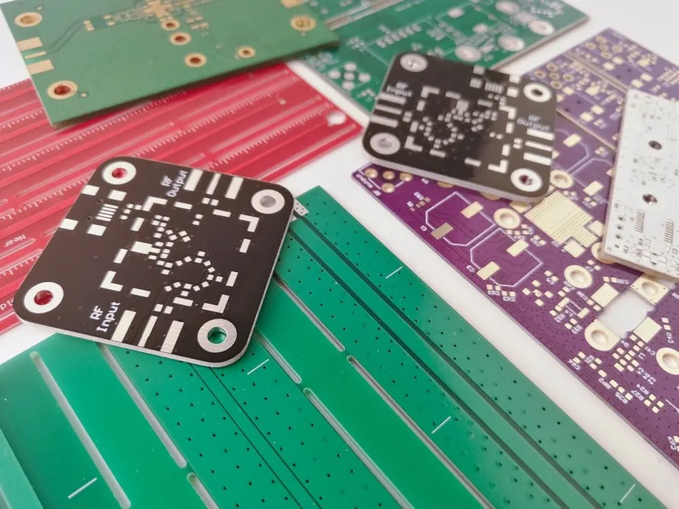
Silk screen printing, also known as legend printing, has long served as the essential layer for marking components, polarity indicators, and assembly instructions on printed circuit boards. Traditionally limited to single colors like white, black, or yellow, this process ensures clear identification during manufacturing and assembly. However, advanced silkscreen color technology is transforming the industry by introducing multi-color capabilities and innovative inks that enhance functionality and aesthetics. These developments align with the demands of high-density interconnect boards and complex electronics driven by 5G, AI, and IoT applications. As factories adopt these techniques, silk screen evolves from a basic labeling tool into a smart, integral part of PCB performance.
Emerging silkscreen color trends focus on precision, sustainability, and integration with digital workflows, promising reduced assembly errors and improved traceability. Electric engineers benefit from these advancements through better visual cues that speed up troubleshooting and maintenance. This article explores the technical principles, innovative silkscreen color techniques, and best practices shaping the future of PCB manufacturing.
What Is Advanced Silkscreen Color Technology and Why It Matters
Advanced silkscreen color technology refers to the next-generation methods and materials used to apply durable, high-contrast markings on PCBs, extending beyond monochrome inks to full-spectrum colors and functional properties. It encompasses digital printing processes that deposit UV-curable inks directly onto the board surface, achieving resolutions up to 1200 dpi and supporting multiple colors simultaneously. This shift addresses limitations of traditional stencil-based screen printing, which struggles with fine details below 0.15 mm stroke width and multi-color setups requiring multiple passes.
In manufacturing, these innovations matter because they boost assembly efficiency by color-coding components, such as using distinct hues for power traces, signal lines, and ground planes, potentially reducing errors by providing immediate visual differentiation. Traceability improves with embedded QR codes as small as 2 mm x 2 mm, scanned in under 0.5 seconds for lifecycle data access. For electric engineers, multi-color silkscreen PCBs enable faster debugging in dense layouts, where traditional legends blur under inspection lights.
Factory-driven insights highlight sustainability gains, as solvent-free UV inks lower VOC emissions to below 10 mg/m3 and support bio-based formulations with over 60% biodegradability. Compliance with industry standards ensures reliability, making these technologies viable for high-volume production in automotive, medical, and consumer sectors.
Technical Principles of Innovative Silkscreen Color Techniques
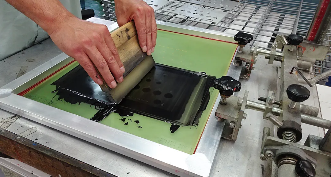
Traditional silk screen printing pushes epoxy-based ink through a mesh stencil onto the PCB, cured via UV or thermal methods, but it limits colors to one per run and requires screen preparation for each design change. Advanced techniques pivot to digital inkjet printing, where piezoelectric heads eject precise droplets of UV-curable ink, curing instantly under LED lamps for sharp edges and no solvents. This allows seamless multi-color layering, with six-color systems producing vibrant graphics without alignment issues common in manual multi-pass printing.
Ink formulations drive these capabilities: standard epoxy inks (50% resin, 45% pigments) withstand 288°C soldering for 10 seconds, but emerging thermochromic variants change color at thresholds like 85°C to signal overheating. Photochromic and phosphorescent inks glow under UV or darkness, ideal for low-light assembly. Resolution hinges on positioning accuracy of ±0.01 mm, enabling 0.076-0.102 mm line widths for high-density boards.
Liquid Photo Imaging (LPI) applies photosensitive liquid, exposed and developed for finer features than stencils, while Direct Legend Printing (DLP) projects ink from CAD data for prototype flexibility. These methods integrate with solder mask application, maintaining 15-35 μm thicknesses without bridging pads, as clearances exceed 0.15 mm per IPC guidelines.
Sustainability principles embed in ink chemistry, with 100% solid UV formulas eliminating waste and halogen-free options meeting environmental regulations. Factory processes leverage automation for quality control, halting on anomalies to uphold consistency.
Emerging Silkscreen Color Trends and Multi-Color Capabilities
Among emerging silkscreen color trends, multi-color silkscreen PCBs stand out, using UV printing to layer vibrant designs, logos, and warnings directly on the board for enhanced brand recognition and user guidance. This technique supports JPG/PNG imports resized to fit without overlapping pads or vias, maintaining non-conductive properties to avoid electrical interference. Digital silkscreen printing accelerates prototyping by eliminating stencils, ideal for low-volume runs with variable data like batch codes.
Thermochromic "sensory silkscreen" represents a functional leap, where inks shift hue to indicate temperature excursions, aiding reliability in power electronics. Glow-in-the-dark phosphors ensure visibility in dark environments, crucial for emergency or automotive PCBs. High-resolution capabilities reach 0.1 mm strokes, surpassing traditional limits for HDI boards with pitches under 0.2 mm.
Integration with AI optimizes placement, predicting error-prone zones for proactive design tweaks. Eco-trends favor bio-based inks from plant resins, balancing adhesion (>3.5 N/cm) and heat resistance (>125°C) with degradability. These trends reduce rework in factories by improving first-pass yields through superior contrast ratios above 4.5:1.
Practical Solutions and Best Practices in Implementation
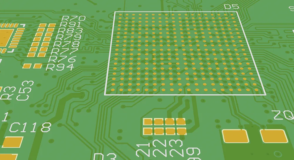
Engineers implementing innovative silkscreen color techniques must prioritize contrast: white or black on green solder masks for 90% recognition accuracy, avoiding yellow/red on similar backgrounds due to blurring. Minimum font heights of 0.8 mm and stroke widths of 0.15 mm ensure legibility, with 6 mil clearances from pads to prevent solder wicking, aligning with IPC-A-600K acceptability criteria.
Design files separate silkscreen layers by color, verifying non-overlap with copper and mask in Gerber outputs. Factories recommend 0.1-0.2 mm ink thickness for durability under 260°C reflow without fading. For multi-color silkscreen PCBs, limit text to 0.8 mm minimum and test under varied lighting for ISO 9241-3 compliance.
Troubleshooting focuses on halo effects from reflective whites, mitigated by matte finishes, and ink adhesion failures addressed via plasma pre-treatment. Sustainability best practices include selecting low-VOC UV inks and recycling screens where applicable. Adhering to IPC-6012E performance specs guarantees qualification across production scales.
Challenges and Factory-Driven Insights
While digital silkscreen printing cuts setup times, challenges like higher upfront costs for non-standard colors (10-20% premium) persist for small batches. Resolution limits in humid environments demand controlled curing to avoid defects. Factories counter with automated inspection, achieving 99% defect detection.
Case insights from high-volume lines show multi-color adoption reducing assembly time by 25% via intuitive coding. Engineers should prototype with DLP for validation before scaling.
Conclusion
The future of silk screen color technology in PCB manufacturing lies in digital methods, multi-color UV printing, and smart inks that elevate legends from passive labels to active aids. Advanced silkscreen color technology and innovative silkscreen color techniques promise efficiency gains, traceability, and sustainability while meeting IPC standards. Electric engineers can leverage emerging silkscreen color trends for robust, user-friendly boards. As factories integrate these, multi-color silkscreen PCBs and digital silkscreen printing will redefine production norms.
FAQs
Q1: What is advanced silkscreen color technology in PCB manufacturing?
A1: Advanced silkscreen color technology involves digital inkjet and UV-curable inks enabling high-resolution, multi-layer color printing on PCBs. It surpasses traditional single-color screen methods by offering 1200 dpi precision and functional properties like thermochromic shifts. Factories use it for better component identification and reduced assembly errors, ensuring compliance with IPC standards for durability.
Q2: How do innovative silkscreen color techniques improve assembly efficiency?
A2: Innovative silkscreen color techniques apply contrasting multi-colors to code signals, power, and grounds, speeding technician workflows. Digital processes eliminate stencil changes, supporting variable designs for prototypes. This results in clearer visuals under inspection, minimizing errors in high-density boards per factory standards.
Q3: What are key emerging silkscreen color trends for electric engineers?
A3: Emerging silkscreen color trends include thermochromic inks for temperature monitoring and glow-in-the-dark variants for low-light use. Multi-color silkscreen PCBs via UV printing enhance traceability with QR codes. Engineers gain from finer 0.1 mm resolutions, aligning with IPC-A-600K for reliable manufacturing.
Q4: Can digital silkscreen printing replace traditional methods entirely?
A4: Digital silkscreen printing offers flexibility for multi-color and fine features without screens, ideal for low-volume and custom runs. It uses instant UV curing for eco-friendly production but may cost more for standards colors in bulk. Factories blend it with screen printing for optimal scalability and IPC-6012E compliance.
References
IPC-A-600K — Acceptability of Printed Boards. IPC, 2020
IPC-6012E — Qualification and Performance Specification for Rigid Printed Boards. IPC, 2017
IPC-SM-840D — Qualification and Performance of Permanent Solder Mask. IPC, 2018


