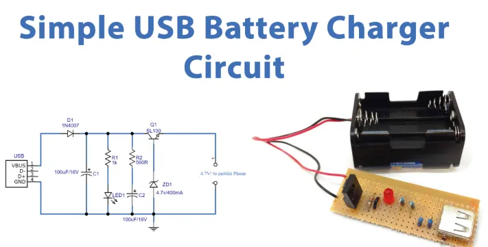
Introduction
Battery chargers represent a critical component in modern electronics, powering everything from consumer devices to electric vehicles. These systems demand robust power handling, precise control signals, and minimal electromagnetic interference to ensure safety and efficiency. Multi-layer PCB design emerges as a cornerstone solution, enabling engineers to integrate high-density circuitry within compact footprints. By stacking multiple conductive layers separated by dielectrics, these boards address the unique challenges of power conversion stages like buck-boost converters and charging controllers. This approach not only optimizes space but also enhances overall system reliability under demanding thermal and electrical conditions. As battery technologies evolve, understanding the role of multi-layer PCBs becomes essential for electric engineers tackling next-generation charger designs.
Why Multi-Layer PCBs Matter in Battery Charger Design
Battery chargers operate in environments with high voltage differentials, rapid switching frequencies, and significant current loads, making single or double-layer boards insufficient. Multi-layer constructions provide the necessary isolation between power paths and sensitive analog signals, preventing crosstalk and noise coupling. This separation is vital for maintaining stable operation during fast charging protocols that can exceed 100A in automotive applications. Moreover, regulatory demands for EMI compliance push designers toward layered architectures that incorporate shielding planes. In essence, multi-layer PCB design allows for scalable solutions that balance performance, size, and manufacturability. Without this capability, chargers would struggle to meet the density requirements of integrated microcontrollers, sensors, and power MOSFETs.
The relevance extends to lifecycle reliability, where multi-layer boards better dissipate heat through dedicated thermal planes and vias. Electric engineers appreciate how these designs facilitate compliance with performance benchmarks for rigid printed boards as outlined in IPC-6012. Ultimately, adopting multi-layer approaches minimizes field failures by improving mechanical stability and electrical integrity over time.
Fundamentals of PCB Stack-up in Multi-Layer Designs
The PCB stack-up defines the arrangement of copper layers, core materials, and prepregs, directly influencing electrical and thermal behavior. In battery chargers, a typical four-layer stack-up might feature signal-ground-power-signal configuration to minimize loop inductance. Engineers must ensure symmetry around the neutral axis to prevent warpage during lamination and reflow processes. Dielectric thickness controls impedance for high-speed signals from communication interfaces like CAN or I2C. Proper stack-up planning also incorporates plane splits judiciously to avoid unintended coupling between power domains.
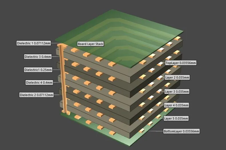
Layer sequencing impacts capacitance between planes, which acts as distributed decoupling for switching regulators. For instance, thin dielectrics between power and ground layers reduce voltage ripple under transient loads. Adhering to generic design guidelines in IPC-2221 helps optimize these parameters for consistent performance. Stack-up decisions thus form the foundation of robust multi-layer PCB design tailored to charger topologies.
Enhancing Signal Integrity in Multi-Layer PCBs
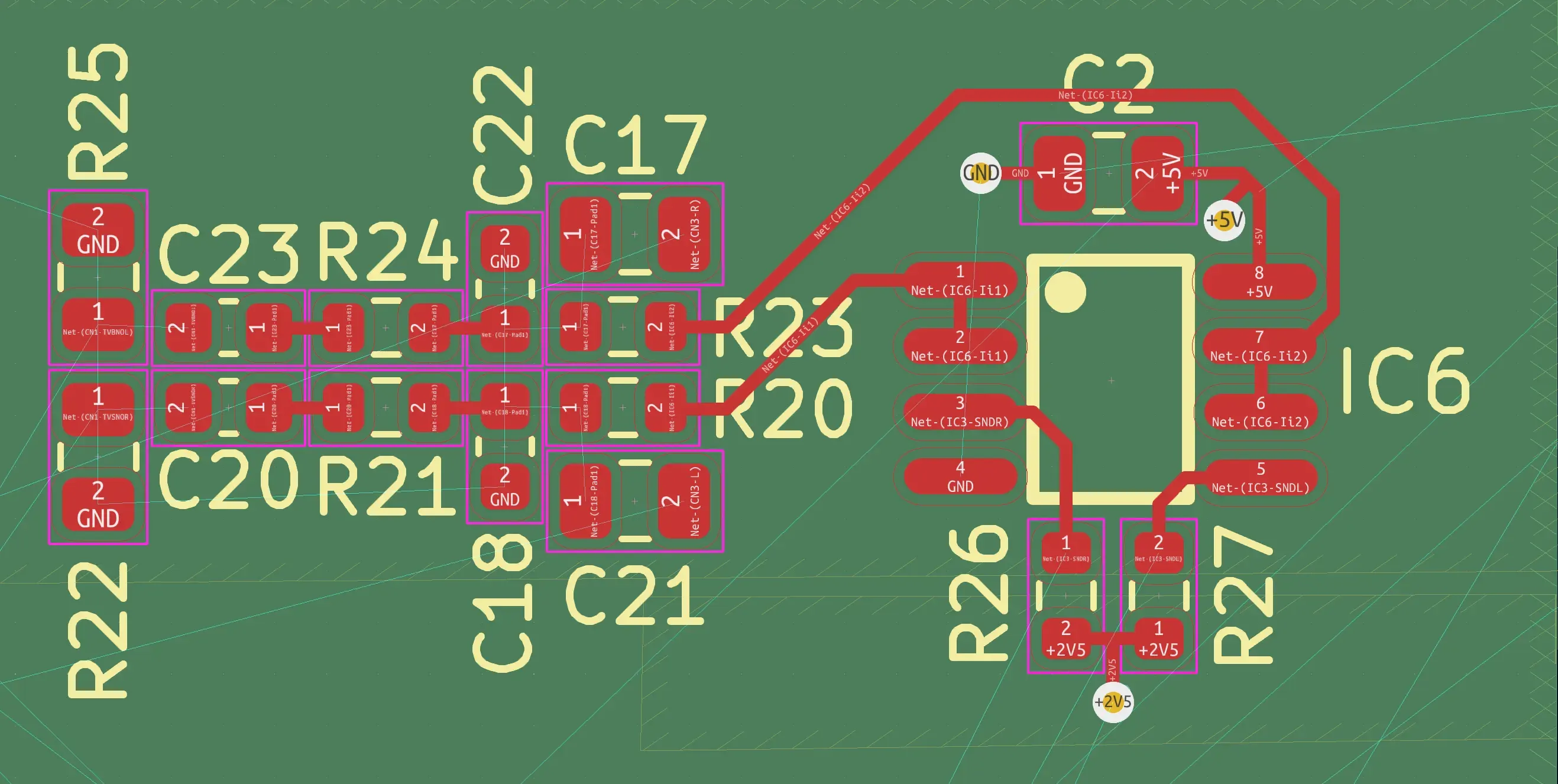
Signal integrity multi-layer strategies rely on controlled impedance traces and reference planes to preserve waveform quality. In battery chargers, microcontroller signals driving PWM for current regulation must resist reflections and jitter. Dedicated inner layers for signals, flanked by ground planes, shorten return paths and suppress common-mode noise. Vias transitioning between layers require stitching grounds nearby to maintain continuity. This layered isolation proves superior to surface routing, where external interference dominates.
Engineers simulate impedance profiles during multi-layer PCB design to match 50-ohm or 100-ohm differentials as needed. Pre-emphasis and equalization become feasible with precise layer alignments. Over long traces, such as those connecting temperature sensors to the controller, multi-layer routing enables length matching without excessive meandering. These practices ensure data integrity for protocols monitoring state-of-charge accurately.
Optimizing Power Distribution in Multi-Layer Designs
Power distribution multi-layer architectures excel by dedicating full planes to high-current paths, slashing resistance and inductance compared to trace-based delivery. Battery chargers benefit from thick copper pours handling tens of amps for input rectification and output regulation. Voltage drops remain minimal across the board, stabilizing FET gate drives and inductor currents. Decoupling capacitors placed near loads leverage plane capacitance for high-frequency bypass.
Current-carrying capacity calculations guide copper weights, with wider planes mitigating hotspots in continuous conduction modes. IPC-2152 provides methodologies for determining safe current densities based on trace geometry and temperature rise. Multi-layer power distribution thus supports efficient thermal management without oversized heatsinks. Engineers layer voltage domains strategically, using split planes connected via low-impedance paths to prevent ground bounce.
EMI Reduction Techniques in Multi-Layer PCBs
EMI reduction multi-layer tactics center on enclosing noisy traces within ground planes, forming Faraday cages that attenuate radiated emissions. Switching converters in chargers generate harmonics up to hundreds of MHz, demanding tight control. Solid ground pours on adjacent layers absorb return currents, minimizing loop areas that act as antennas. Guard traces and moats further isolate sensitive analog sections from digital noise.
Cross-talk diminishes as signals propagate between planes rather than on the surface. Engineers prioritize via fencing around high-speed edges to contain fields. Compliance testing reveals how multi-layer shielding outperforms simpler boards by 10-20 dB in critical bands. These layered defenses ensure chargers pass emissions standards without bulky filters.
Key Design Considerations and Challenges
While advantageous, multi-layer PCB design introduces complexities like interlayer registration tolerances and via reliability under thermal cycling. Battery chargers experience wide temperature swings from ambient to over 100°C during fast charge, stressing drill-plated vias. Warpage control demands balanced stack-ups with matched prepreg stacks. Cost escalates with layer count, prompting trade-offs between performance and budget.
Fabrication yields drop if aspect ratios exceed 10:1 for blind vias, common in dense chargers. Signal skew across layers requires careful routing hierarchies. Engineers mitigate these by iterating simulations early and validating prototypes with cross-sections. Material selection influences CTE mismatch, critical for long-term solder joint integrity.
Best Practices for Multi-Layer PCB Implementation in Battery Chargers
Start with stack-up planning using symmetry and plane pairing for optimal impedance and PDN. Route high-current paths on inner layers to leverage thicker foils, reserving surfaces for components. Implement thermal reliefs and embedded vias for heat spreading from power devices. Perform SI/PI/EMI co-simulations to verify before layout freeze.
Collaborate with fabricators on DFM checks for drill sizes and panelization. Prototype with flying probe tests to catch opens in dense nets. Document layer assignments clearly for assembly teams. These steps yield reliable multi-layer boards ready for high-volume production.
Conclusion
Multi-layer PCBs transform battery charger design by delivering superior signal integrity multi-layer control, efficient power distribution multi-layer handling, and effective EMI reduction multi-layer shielding. PCB stack-up optimization underpins these gains, balancing density with reliability. Electric engineers must weigh advantages against fabrication challenges to realize compact, high-performance chargers. Adopting structured approaches aligned with industry standards ensures designs meet demanding electrical and thermal requirements. As charging speeds increase, multi-layer innovations will remain pivotal for advancing portable and EV power systems.
FAQs
Q1: What role does PCB stack-up play in multi-layer PCB design for battery chargers?
A1: PCB stack-up determines layer sequencing, dielectric spacing, and plane assignments critical for impedance control and thermal dissipation. In chargers, symmetric stack-ups prevent warpage while pairing power-ground planes lowers inductance for stable regulation. Engineers calculate capacitance for decoupling and verify via transitions to maintain integrity. This foundational element directly impacts overall multi-layer PCB design success.
Q2: How does signal integrity multi-layer improve performance in high-speed charger circuits?
A2: Signal integrity multi-layer uses reference planes to control trace impedance and minimize crosstalk in PWM and sensor signals. Ground stitching reduces return path inductance, preserving edges for accurate control loops. Simulations guide routing to match lengths and avoid stubs. Resulting cleaner waveforms enhance efficiency and reduce error rates in battery management systems.
Q3: Why prioritize power distribution multi-layer in battery charger layouts?
A3: Power distribution multi-layer employs dedicated planes for low-resistance delivery, vital for high-current stages like rectification. This cuts voltage droop and supports parallel paths without bottlenecks. IPC-2152 aids in sizing for temperature limits. Enhanced PDN stability boosts converter efficiency and component longevity under load.
Q4: What are effective EMI reduction multi-layer strategies for chargers?
A4: EMI reduction multi-layer involves enclosing signals between ground planes to confine fields and shorten loops. Via fences and solid pours attenuate harmonics from switchers. Split planes with stitching prevent leakage. These techniques ensure compliance without external shields, optimizing space in compact designs.
References
IPC-2221C — Generic Standard on Printed Board Design. IPC, 2023
IPC-6012F — Qualification and Performance Specification for Rigid Printed Boards. IPC, 2023
IPC-2152B — Standard for Determining Current Carrying Capacity in Printed Board Design. IPC, 2020


