Introduction
Smart home devices, such as sensors, thermostats, and wireless hubs, operate in environments where reliable battery performance is essential. These devices demand low power PCB design techniques to extend operational time between charges or replacements. Engineers face challenges in balancing functionality with minimal energy draw, especially as device complexity increases with integrated sensors and connectivity features. Effective PCB design directly impacts overall system efficiency, reducing heat generation and enabling smaller form factors. This guide explores proven strategies for achieving energy efficiency in PCB layouts tailored to smart home applications. By focusing on layout optimization, component choices, and power delivery, designers can create robust solutions that meet user expectations for longevity.
Understanding Low-Power PCB Design and Its Importance
Low-power PCB design refers to the systematic approach of minimizing energy consumption across the board level while maintaining signal integrity and reliability. In smart home devices, where batteries often power intermittent operations like motion detection or data transmission, every microamp counts toward extending device uptime. Poor design choices, such as inefficient routing or suboptimal component placement, lead to higher quiescent currents and faster drain rates. This matters because consumers expect devices to last months or years on a single battery, influencing market competitiveness. Adopting low power PCB design techniques ensures compliance with energy regulations and supports sustainable electronics. Ultimately, these methods allow engineers to prioritize performance without compromising on power budgets.
Core Principles of Low Power PCB Design Techniques
The foundation of low power PCB design techniques lies in reducing parasitic effects and optimizing current paths. Engineers start by minimizing trace resistance through wider power traces, which lower voltage drops under load. Ground planes provide return paths that reduce inductance, stabilizing voltage rails during transients. Separating analog and digital sections prevents noise coupling that could trigger unnecessary switching activity. Decoupling capacitors placed close to IC pins filter high-frequency noise, ensuring clean power delivery. These principles form the basis for scalable designs in battery-operated smart home systems.
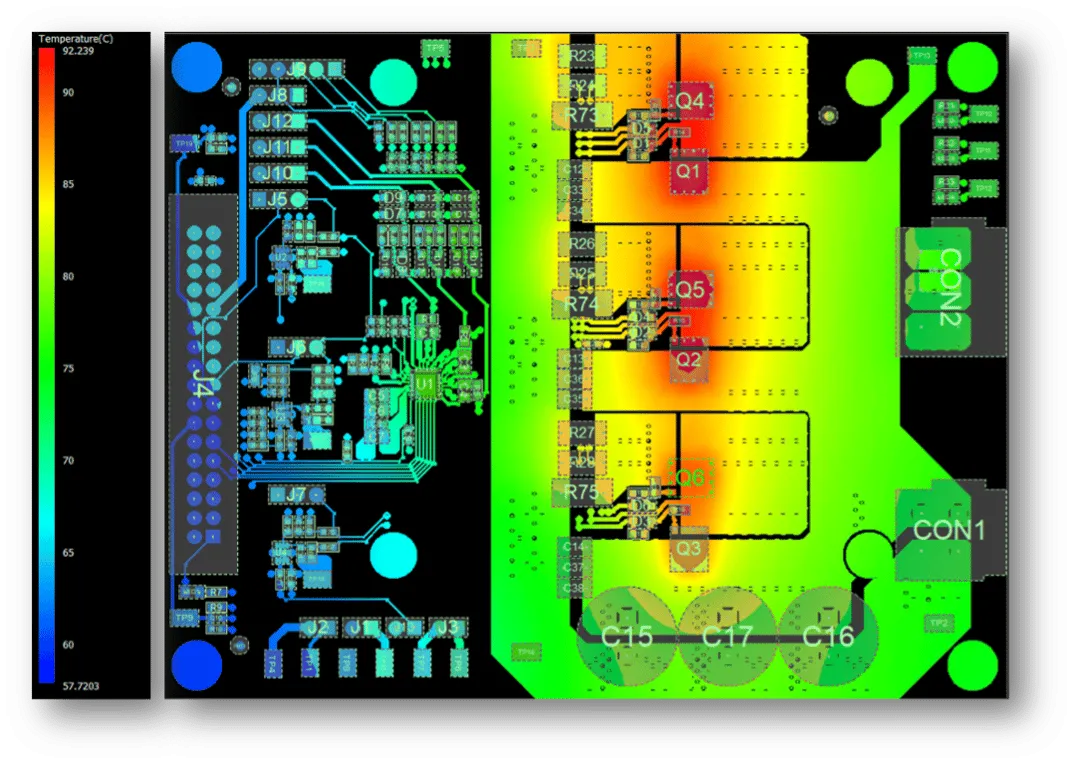
Layer stackup plays a critical role in thermal management and signal isolation. Using dedicated power and ground planes reduces loop areas, minimizing electromagnetic interference. Thinner dielectrics between planes lower impedance at high frequencies. Controlled impedance traces for sensitive signals maintain data integrity without excess power. Vias must be strategically placed to avoid bottlenecks in current flow. By adhering to these structured approaches, designs achieve lower overall power dissipation.
Battery Life Optimization in PCB Design
Battery life optimization PCB strategies focus on holistic power profiling from schematic to layout. Engineers analyze duty cycles to identify peak and average currents, guiding trace width calculations. Sleep modes in microcontrollers require careful power domain isolation to prevent leakage from active sections. Efficient regulators convert battery voltage with minimal losses, preserving capacity over discharge cycles. Parasitic loads from unused pins or floating inputs must be eliminated through proper pull-up or pull-down resistors. These optimizations can significantly extend runtime in smart home sensors that wake periodically.
Layout contributes directly to battery life optimization PCB efforts by reducing IR drops. Power traces routed with minimal bends maintain low resistance, ensuring uniform voltage across loads. Thermal vias under hot components dissipate heat without relying on active cooling, which would consume extra power. Board edge effects, like battery connector placement, influence efficiency; positioning them near regulators shortens high-current paths. Simulation tools verify these choices pre-prototype, catching issues early. Comprehensive optimization yields devices that operate reliably for extended periods.
Selecting Energy Efficient Components
Energy efficient components form the cornerstone of low-power designs, starting with microcontrollers featuring deep sleep currents below microamp levels. Sensors with low standby power suit intermittent smart home tasks like environmental monitoring. Passives, such as capacitors with low equivalent series resistance, minimize losses in filtering networks. Logic families with rail-to-rail operation reduce switching thresholds, cutting dynamic power. Engineers evaluate datasheets for quiescent current specs under real operating conditions. Matching component efficiency to application needs prevents overdesign and wasted energy.
Component footprint and thermal performance also matter for energy efficient components. Smaller packages reduce parasitic capacitance, aiding faster switching with less charge. Low thermal resistance materials handle dissipation without derating efficiency. Voltage regulators with high power supply rejection ratio maintain clean rails despite battery variations. Grouping components by power domain simplifies management. Thoughtful selection ensures the PCB supports ultra-low power modes effectively.
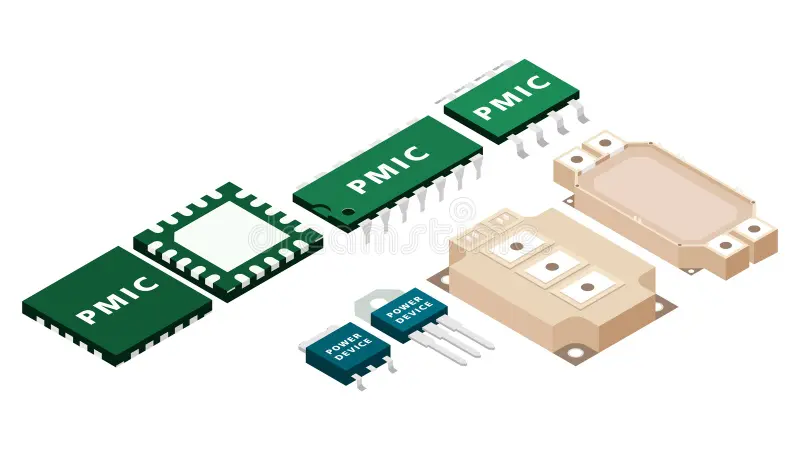
Integrating Power Management ICs Effectively
Power management ICs serve as gatekeepers for energy in smart home PCBs, handling conversion, sequencing, and protection. Buck converters outperform linear regulators in efficiency for stepping down battery voltages, especially at light loads. These ICs include features like low dropout modes and soft-start to limit inrush currents. Placement near loads reduces trace losses, with input capacitors sized for ripple suppression. Feedback loops must use stable resistors to avoid oscillations that waste power. Proper integration maximizes battery utilization across discharge profiles.
Thermal considerations guide power management ICs layout to prevent efficiency roll-off. Adequate copper pours act as heatsinks, spreading heat evenly. Multiple vias connect to inner planes for better dissipation. Sequencing ensures peripherals power up without glitches, preserving stability. Monitoring circuits within ICs enable dynamic adjustments based on load. These practices align with low power PCB design techniques for sustained performance.
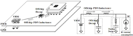
Optimizing the PCB Power Distribution Network
The PCB power distribution network delivers stable voltage with minimal impedance, critical for low-power operation. Wide planes or mesh grids provide low resistance paths, supporting transient demands from wireless modules. Decoupling strategies use capacitors at multiple frequencies: bulk for low, ceramic for high. Via stitching along power edges reduces inductance between layers. Plane splits must include bridges to avoid isolated islands. Target impedance profiles guide PDN design, ensuring margins under worst-case loads.
Simulation refines the PCB power distribution network by modeling frequency-dependent behavior. Engineers iterate on via density and capacitor values to flatten impedance curves. Return path integrity prevents ground bounce that triggers resets. For multi-rail systems, careful partitioning isolates noise. These optimizations support energy efficient components by providing clean power. A well-designed PDN enhances overall system reliability in battery-powered devices.
Best Practices and Standards Compliance
Implementing best practices involves iterative verification of low power PCB design techniques. Prototype testing measures actual consumption against simulations, refining layouts. Automated checks enforce minimum trace widths and clearance rules. Multi-stage reviews catch leakage paths early. Documentation traces decisions back to requirements, aiding future iterations.
Compliance with industry standards ensures manufacturability and reliability. IPC-2221B provides guidelines for conductor sizing and spacing in power sections, preventing overheating. J-STD-001GS outlines soldering requirements for low-power assemblies, minimizing defects that cause shorts. IPC-2152B offers current-carrying capacity data for traces, supporting accurate PDN planning. These standards, applied non-adjacently across design phases, elevate quality without excess power use.
Conclusion
Low-power PCB design for smart home devices integrates component selection, layout precision, and PDN optimization to maximize battery life. Techniques like wide traces, efficient regulators, and plane utilization reduce losses systematically. Engineers benefit from structured approaches that balance performance and efficiency. Adhering to standards reinforces these efforts, yielding reliable products. As devices evolve, these principles remain foundational for innovation.
FAQs
Q1: What are the main low power PCB design techniques for extending battery life in smart home devices?
A1: Low power PCB design techniques include using wide power traces to minimize resistance, placing decoupling capacitors near ICs, and separating analog from digital sections to reduce noise. Ground planes lower inductance for stable returns. Efficient regulators replace linear types, and sleep mode isolation prevents leakage. These steps optimize current paths and reduce quiescent draw, directly boosting runtime.
Q2: How do energy efficient components impact battery life optimization PCB strategies?
A2: Energy efficient components with low quiescent currents and minimal leakage suit battery life optimization PCB efforts by lowering baseline consumption. Microcontrollers with deep sleep modes and low-ESR capacitors reduce losses during operation and idle. Selection based on datasheet specs under real loads ensures matching to duty cycles. Proper footprints minimize parasitics, enhancing overall efficiency.
Q3: Why is the PCB power distribution network crucial in power management ICs integration?
A3: The PCB power distribution network ensures low-impedance delivery to power management ICs, preventing voltage droops during transients. Strategic via placement and plane usage support high-frequency stability. This setup allows ICs to maintain efficiency without ripple-induced losses. Clean PDNs enable features like dynamic voltage scaling, optimizing for varying smart home loads.
Q4: What role do industry standards play in low power PCB design techniques?
A4: Industry standards like IPC-2221B guide trace sizing and thermal management in low power PCB design techniques, ensuring reliability. They provide data for current capacity without excess width that adds capacitance. Compliance verifies designs against proven criteria, reducing field failures. This structured adherence supports scalable, efficient smart home solutions.
References
IPC-2221B - Generic Standard on Printed Board Design. IPC, 2009
IPC-2152B - Standard for Determining Current Carrying Capacity in Printed Board Design. IPC, 2009
J-STD-001GS - Requirements for Soldered Electrical and Electronic Assemblies. IPC, 2020


