Introduction
Spacecraft electronics rely on printed circuit boards (PCBs) to manage power distribution, data processing, and communication in unforgiving environments. PCB design software plays a pivotal role in creating boards that withstand radiation, extreme temperatures, and mechanical stresses. Electrical engineers working on space projects must select tools that support rigorous design rules and simulations tailored to these conditions. This guide explores the essential features, challenges, and best practices for PCB design software in space applications. By focusing on reliability and performance, engineers can ensure mission success where failure is not an option. Understanding these tools helps optimize designs from concept to fabrication.
Why Spacecraft Electronics Demand Specialized PCB Design Software
Space missions expose electronics to conditions far beyond terrestrial standards, including cosmic radiation, thermal cycling from -150°C to +125°C, and launch vibrations exceeding 20g. Standard PCB design tools often fall short, lacking advanced analysis for signal integrity under radiation or thermal management in vacuum. Specialized software enables engineers to model these effects early, reducing iteration costs that can reach millions per redesign. Compliance with standards like IPC-6012DS for space-qualified rigid boards becomes seamless through built-in design rule checks. Moreover, the software must handle complex multilayer stackups necessary for high-density interconnects in compact satellite systems. Ultimately, the right tool bridges schematic capture, layout, and verification for zero-defect outcomes.
Key Challenges in Spacecraft PCB Design
Radiation poses the primary threat, causing total ionizing dose (TID) degradation and single-event effects (SEE) that flip bits or latch components. Thermal extremes lead to coefficient of thermal expansion (CTE) mismatches, risking delamination or solder joint cracks during cycling. Vibration and shock during launch demand robust mechanical designs, with resonances amplifying stresses on traces and vias. Vacuum environments exacerbate outgassing from materials, potentially contaminating optics or sensors. Electromagnetic interference (EMI) from high-speed signals requires precise impedance control and shielding. Design software for the aerospace PCB must simulate these interactions to predict failures before prototyping.
High-reliability requirements amplify these issues, as spacecraft PCBs operate without maintenance for years. Engineers face trade-offs in material selection, balancing low outgassing with electrical performance. Power integrity analysis for spacecraft electronics becomes critical for distributed systems handling kilowatts in propulsion controls. Miniaturization for CubeSats squeezes traces into sub-mil widths, heightening crosstalk risks. Software with integrated physics-based solvers addresses these by coupling electrical, thermal, and structural analyses.
Essential Features of the Best PCB Design Software for Space Applications
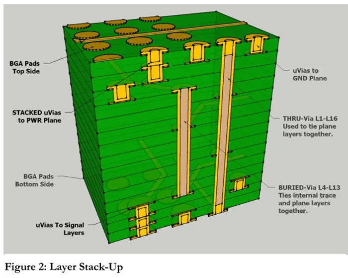
The best PCB design software for space applications offers multilayer support up to 50 layers or more, with automated stackup generators optimizing for symmetric builds to minimize warpage. Constraint-driven routing enforces controlled impedance for differential pairs, essential for gigabit transceivers enduring radiation-induced noise. Signal integrity (SI) tools simulate eye diagrams, crosstalk, and reflections under varying temperatures, predicting bit error rates. Power integrity (PI) analysis models DC drops and AC noise across voltage planes, crucial for rad-hard power supplies.
Thermal simulation integrates with layout, mapping heat from components to board-level dissipation via vias and planes. Mechanical stress analysis evaluates vibration response, flagging weak points in via farms or trace bends. 3D modeling verifies fit within chassis, accounting for conformal coatings that add thickness. Design rule checks (DRC) align with IPC-2221 generic standards, flagging violations like inadequate annular rings or spacing. For EMI/EMC, field solvers compute return paths and shielding effectiveness.
Advanced verification includes automated netlist comparisons and fab output generation for HDI via-in-pad structures. Integration with component libraries for space-qualified parts streamlines selection. Real-time collaboration features aid distributed teams on large projects like interplanetary probes.
PCB Design Software Comparison
When comparing PCB design software, prioritize tools with native SI/PI engines over those relying on external plugins, as seamless workflows reduce errors in high-stakes space designs. Enterprise solutions excel in handling massive boards with thousands of components, offering hierarchical designs for modular spacecraft systems. Free PCB design software for hobbyists suits CubeSat prototypes but lacks deep simulation, making it unsuitable for flight hardware without supplementation.
- Layer Count Support — Basic Tools: Up to 16; Advanced Space-Optimized Tools: 50+ with blind/buried vias
- SI/PI Simulation — Basic Tools: Time-domain basic; Advanced Space-Optimized Tools: Full-wave 3D + radiation models
- Thermal/Mechanical Analysis — Basic Tools: 2D steady-state; Advanced Space-Optimized Tools: Coupled transient + vibration
- DRC for Standards — Basic Tools: Generic IPC Class 2; Advanced Space-Optimized Tools: IPC-6012DS space addendum
- Cost — Basic Tools: Free/open-source; Advanced Space-Optimized Tools: Subscription-based enterprise
Basic tools appeal to hobbyists prototyping ground stations, while advanced ones dominate professional space workflows. Hybrid approaches combine free schematic capture with paid layout for cost efficiency.
Best Practices Using PCB Design Software for Space Applications
Start with a robust schematic incorporating rad-hard components, using the software's library manager to verify parameters like TID tolerance. Define design rules early, setting trace widths for 20% current margins and via sizes per J-STD-001 space addendum for solder joint reliability. Optimize stackups for balanced copper distribution, placing power/ground planes adjacent to signal layers to suppress EMI.
Employ length-matching for clocks and data buses to maintain timing under thermal expansion. Insert thermal vias under hot components, simulating dissipation to keep junctions below 125°C. Route sensitive analog signals away from digital noise, using guard traces and stitching vias for shielding. Perform iterative SI sweeps, adjusting terminations for clean eyes at worst-case corners.
Validate mechanically by exporting to FEA tools, checking natural frequencies above launch profiles. Generate panelized arrays for qualification testing, ensuring fiducials for alignment. Document deviations with rationale, maintaining traceability for audits.
For free PCB design software for hobbyists, focus on DRC enforcement and export to simulators, bridging to professional verification. Always prototype and test iteratively, as simulations approximate real physics.
Conclusion
Selecting the best PCB design software for space applications hinges on comprehensive simulation, standards compliance, and workflow efficiency. Engineers must tackle radiation, thermal, and mechanical challenges through feature-rich tools that predict real-world performance. A thoughtful PCB design software comparison reveals advanced options outperforming basics in reliability. Adhering to practices like constraint-driven design and coupled analyses ensures mission-ready boards. As space exploration accelerates, mastering these tools empowers innovation in electronics. Future designs will leverage AI-assisted routing for even tighter margins.
FAQs
Q1: What makes the best PCB design software for space applications stand out?
A1: Advanced space PCB design demands integrated signal integrity, thermal, and mechanical simulations alongside DRC for IPC-6012DS. These tools handle multilayer HDI with impedance control, outperforming basic software in predicting radiation effects and vibration response. Electrical engineers benefit from real-time 3D verification, reducing prototypes by validating designs upfront. Free options suit initial concepts but require supplements for full qualification.
Q2: How does PCB design software comparison help in space projects?
A2: Comparing software highlights differences in simulation depth, layer support, and standards integration like J-STD-001. Enterprise tools offer PI analysis for power systems, while hobbyist free PCB design software excels in accessibility for prototypes. Prioritize native physics solvers for accurate EMI modeling in vacuum. This ensures selection aligns with mission reliability needs.
Q3: Can free PCB design software for hobbyists handle spacecraft electronics?
A3: Free tools provide schematic and basic layout for hobbyist CubeSats but lack advanced SI/PI for space extremes. They enforce generic DRC, useful for ground support but not flight hardware without external validation. Engineers pair them with simulators for thermal checks. For professional use, upgrade to feature-complete options.
Q4: What role do standards play in space PCB design software?
A4: Standards like IPC-2221 guide trace spacing and materials in software DRC, ensuring space qualification. J-STD-001 addendums enforce solderability under vibration. Integrated checks automate compliance, minimizing human error. This streamlines from design to testing.
References
[Reference 1] IPC-6012DS - Space and Military Avionics Applications Addendum to IPC-6012D, Qualification and Performance Specification for Rigid Printed Boards. IPC.
[Reference 2] J-STD-001GS - Space and Military Applications Electronic Assemblies. IPC/JEDEC.
[Reference 3] IPC-2221 - Generic Standard on Printed Board Design. IPC.


