Introduction
In modern electronics, printed circuit boards (PCBs) form the backbone of virtually every device, from consumer gadgets to industrial systems. Ensuring their quality and reliability demands rigorous test and measurement strategies integrated early in the design phase. Poor testing can lead to field failures, costly rework, and compromised performance, especially as boards grow denser and faster. This guide explores key aspects like PCB design for testability (DFT), signal integrity testing in PCB design, impedance testing for PCB, functional testing of PCBs, and in-circuit testing (ICT) explained. By understanding these elements, electrical engineers can minimize defects and optimize production yields. Adopting structured testing aligns designs with industry expectations for durability and functionality.
Test and measurement go beyond basic continuity checks; they verify electrical, mechanical, and thermal integrity under real-world conditions. High-speed signals, fine-pitch components, and multilayer stacks amplify risks like crosstalk and warpage. Proactive approaches catch issues before assembly, saving time and resources. This article provides logical explanations, best practices, and engineering insights to elevate your PCB workflows.
Why Test and Measurement Matter in PCB Design
Test and measurement in PCB design directly impact product lifespan and compliance. As signal speeds exceed gigahertz ranges and component densities increase, unaddressed issues like impedance mismatches cause signal degradation. Early detection prevents propagation of flaws from design to fabrication and assembly. Engineers must prioritize these processes to meet performance specs and reduce warranty claims.
Factory-driven insights reveal that inadequate testing accounts for a significant portion of assembly rejects. Standards like IPC-6012 outline qualification criteria that emphasize electrical and mechanical performance. Integrating tests ensures boards withstand environmental stresses such as vibration and thermal cycling. Ultimately, robust testing bridges design intent with reliable manufacturing outcomes.
Beyond cost savings, comprehensive testing fosters innovation in high-reliability sectors like aerospace and automotive. It validates assumptions in simulations, confirming real-world behavior. Neglecting this step risks systemic failures that undermine system-level integrity.
PCB Design for Testability (DFT)
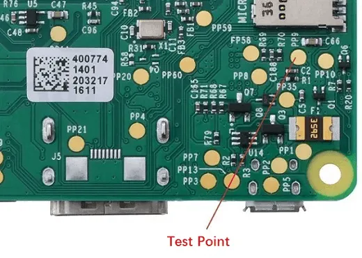
PCB design for testability (DFT) incorporates features that facilitate efficient verification during manufacturing. Core principles include placing accessible test points on nets, avoiding hidden vias, and ensuring probe clearance around components. DFT minimizes test escapes by enabling boundary-scan protocols like JTAG for digital logic. Engineers allocate space for these elements without compromising routing density.
Logical planning starts with netlist analysis to identify critical nodes for probing. Test points should span high-speed lines, power rails, and analog sections. Component orientation aids uniform fixture access, reducing custom adaptations. This structured approach aligns with production realities, streamlining in-circuit and functional tests.
DFT also addresses shielding and grounding to isolate test signals from operational noise. Factory practices favor designs with at least 20% of nets probed for coverage. By embedding these strategies, engineers achieve higher fault coverage and faster debug cycles.
Signal Integrity Testing in PCB Design
Signal integrity testing in PCB design evaluates how signals maintain quality across traces and vias. Key concerns include reflections, crosstalk, and attenuation, which distort timing and voltage levels. Time-domain reflectometry (TDR) and frequency-domain analysis using vector network analyzers (VNAs) quantify these effects. Engineers launch tests post-layout to validate stackup and routing choices.
Pre-layout simulations predict issues, but physical testing confirms fabrication variances like etch tolerances. Eye diagram analysis reveals jitter and overshoot in high-speed interfaces. Proper reference planes and length matching mitigate common degradation sources. These measurements guide iterative refinements for clean signal propagation.
Advanced setups incorporate oscilloscopes with de-embedding to isolate board contributions from fixtures. Correlation between simulation and measurement refines future designs. Consistent application ensures compliance with performance margins across production lots.
Impedance Testing for PCB
Impedance testing for PCB verifies controlled characteristic impedance on transmission lines, crucial for high-frequency signals. Discontinuities from vias or bends cause reflections that degrade data rates. IPC-2141 provides design guidelines for calculating microstrip and stripline impedances based on stackup parameters. TDR excels here, displaying impedance profiles along traces with picosecond resolution.
Test procedures involve calibrating probes to the board reference, then scanning for deviations beyond tolerance, typically 10% or tighter. VNA sweeps reveal S-parameters for insertion loss and return loss. Engineers adjust trace widths and dielectric thicknesses pre-fab to hit targets. Post-etch verification catches plating variations or material inconsistencies.
Routine testing integrates with bare-board electrical checks per IPC-9252 protocols. It ensures signal paths behave predictably in assembled systems. Mastering these techniques optimizes high-speed PCB performance.
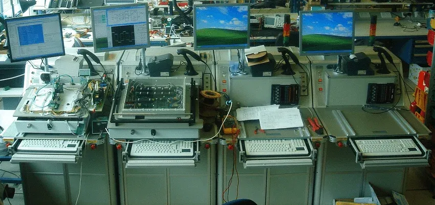
In-Circuit Testing (ICT) Explained
In-circuit testing (ICT) explained involves probing assembled PCBs to verify component values, solder joints, and basic connectivity. Bed-of-nails fixtures press spring-loaded pins against test points, applying stimuli like voltage and current. It detects opens, shorts, wrong polarity, and out-of-tolerance parts with high throughput. DFT features like dedicated pads enhance pin access and accuracy.
Programming derives from Gerber and BOM data, generating node lists for automated execution. Guardian nodes isolate sections to prevent back-driving sensitive ICs. Parametric measurements include resistance, capacitance, and diode checks. ICT coverage often exceeds 90% for accessible nets, complementing visual inspections.
Limitations arise with densely packed BGAs, where x-ray assists shadowed areas. Hybrid flying-probe systems offer flexibility for low-volume runs. Regular fixture maintenance preserves pin integrity and repeatability.
Functional Testing of PCBs
Functional testing of PCBs simulates end-use conditions to confirm overall system operation. Unlike ICT's component focus, it exercises interactions between circuits, firmware, and interfaces. Testers apply inputs via connectors, monitoring outputs for timing, levels, and protocols. This validates design specs under power-up, load, and stress scenarios.
Custom jigs replicate enclosures, including thermal and mechanical loads. Boundary-scan chains enable at-speed testing of digital blocks. Analog sections require stimulus-response verification with precision sources. High fault coverage demands comprehensive vectors covering edge cases.
Post-functional analysis logs failures for root-cause triage, often linking to upstream processes. It serves as the final gate before system integration. Engineers prioritize critical paths to balance test time and depth.
Best Practices for Test and Measurement
Integrate DFT from schematic capture, assigning test strategies per net class. Collaborate with fabricators on stackup for impedance control. Standardize fixtures with modular bases for variants. Calibrate equipment per manufacturer specs before runs.
Layer test escapes by combining ICT, functional, and burn-in. Document thresholds aligned with product classes. Analyze yield data to refine designs iteratively. These practices boost reliability while controlling costs.
Troubleshooting Common Test Failures
Intermittent opens often trace to via cracks or pad lifts; inspect with cross-sectioning. Impedance spikes indicate etch undercuts; review fab drawings. Signal distortion points to crosstalk; add stitching vias. Systematic DFT resolves most issues preemptively.
Conclusion
Mastering test and measurement elevates PCB design from adequate to exceptional. DFT, signal integrity testing, impedance verification, ICT, and functional testing form a cohesive strategy for quality assurance. Logical implementation per standards ensures reliable boards. Electrical engineers gain confidence in designs that perform consistently in the field. Prioritize these elements for superior outcomes.
FAQs
Q1: What is PCB design for testability (DFT), and why incorporate it early?
A1: PCB design for testability (DFT) embeds features like test points and scan chains to simplify verification. Early integration reduces manufacturing defects and test times by providing clear access for probes. It enhances fault isolation, improving yields in high-volume production. Factory insights confirm DFT cuts debug efforts significantly.
Q2: How does signal integrity testing in PCB design identify issues?
A2: Signal integrity testing in PCB design uses TDR and eye diagrams to detect reflections and jitter. It measures waveform quality against specs, pinpointing routing flaws. Regular checks validate high-speed performance post-fabrication. This structured approach prevents field failures.
Q3: What methods are used for impedance testing for PCB?
A3: Impedance testing for PCB employs TDR for time-based profiles and VNAs for frequency sweeps. Calibration ensures accuracy, with tolerances per design goals. It confirms trace integrity for signal fidelity. Essential for multilayer high-speed boards.
Q4: Explain in-circuit testing (ICT) and its role in functional testing of PCBs.
A4: In-circuit testing (ICT) explained probes assemblies for component and joint integrity using fixtures. It precedes functional testing of PCBs, which verifies system behavior. Together, they provide layered assurance. ICT catches basics, enabling focused functional validation.
References
IPC-9252B — Guidelines and Requirements for Electrical Testing of Unpopulated Printed Boards. IPC, 2016
IPC-2141A — Design Guide for High-Speed Controlled Impedance Circuit Boards. IPC, 2002
IPC-6012DS — Qualification and Performance Specification for Rigid Printed Boards. IPC, 2020
IPC J-STD-001G — Requirements for Soldered Electrical and Electronic Assemblies. IPC, 2017


