Introduction
Railway signaling systems form the backbone of safe and efficient rail operations, relying heavily on printed circuit boards (PCBs) to process signals, control switches, and monitor tracks. These PCBs operate in demanding environments characterized by extreme temperatures, vibrations, and confined spaces that exacerbate heat buildup. Effective thermal management ensures component longevity, prevents signal errors, and maintains compliance with reliability requirements. In railway electronics cooling, strategies like PCB heat dissipation techniques become critical to avoid hotspots that could lead to failures. This article explores proven methods tailored for railway signaling PCBs, from design principles to implementation. Engineers designing these boards must prioritize heat transfer mechanisms to sustain performance under pressure.
Why Thermal Management Matters in Railway Signaling PCBs
Railway signaling PCBs handle power-hungry components such as microcontrollers, power relays, and sensors, generating significant heat during continuous operation. Elevated temperatures accelerate material degradation, increase leakage currents, and reduce mean time between failures, directly impacting safety-critical functions. In trackside enclosures or onboard systems, ambient temperatures can swing from sub-zero winters to scorching summers, compounding internal heat. Poor PCB heat dissipation leads to delamination, solder joint cracks, or trace electromigration, all of which compromise signal integrity. For electric engineers, understanding railway electronics cooling is essential to meet operational uptime demands exceeding 99.9%. Proactive thermal strategies not only extend PCB lifespan but also optimize energy efficiency in power-constrained railway setups.
Heat Generation and Transfer Principles in PCBs
Heat in railway signaling PCBs arises primarily from Joule heating in copper traces, dielectric losses in substrates, and power dissipation from active components like voltage regulators and transceivers. Conduction through copper layers and vias dominates in multilayer boards, while convection from air or forced airflow aids surface cooling. Radiation plays a minor role unless temperatures exceed 100 degrees Celsius. Fourier's law governs conductive heat flow, where thermal conductivity of materials dictates efficiency; standard FR-4 substrates offer around 0.3 W/mK, limiting dissipation. In railway applications, transient loads from signal processing spikes create localized hotspots, necessitating uniform spreading. Engineers must model these dynamics to predict temperature rises accurately.
PCB Heat Dissipation Techniques for High-Reliability Applications
Effective PCB heat dissipation starts with copper pour areas and ground planes that spread heat laterally across the board. Thick copper layers, up to 4 oz per square foot, enhance conductivity and lower trace resistance, reducing I-squared-R losses. Component placement keeps high-power devices away from sensitive analog circuits, minimizing thermal crosstalk. Vents or cutouts in enclosures promote natural convection, crucial for railway electronics cooling in sealed cabinets. Filled vias under pads improve vertical heat paths without compromising solderability. These techniques collectively lower junction temperatures, preserving performance in vibration-prone environments.
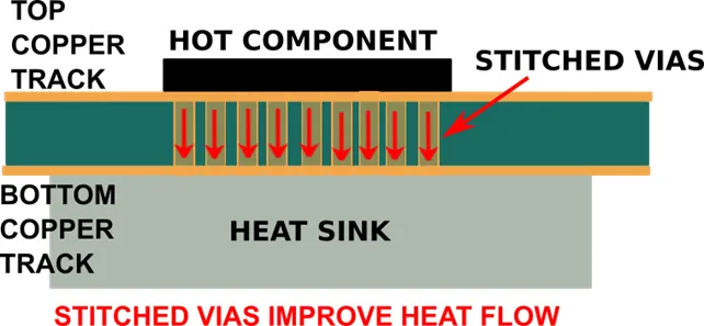
Leveraging Thermal Vias for Efficient Heat Transfer
Thermal vias consist of arrays of plated through-holes connecting surface pads to inner copper planes, creating low-impedance thermal conduits. Typically 0.3 mm diameter with 1 mm pitch, they transfer heat from component bottoms to a heat sink or chassis. Filling vias with conductive epoxy prevents solder wicking during assembly, maintaining reliability. In multilayer railway PCBs, stacking vias across planes multiplies conductance, often achieving 10-20 times better dissipation than solid copper alone. Placement under ICs or resistors forms "via farms" that equalize temperatures. Designers balance via density with fabrication costs and signal integrity concerns like crosstalk.
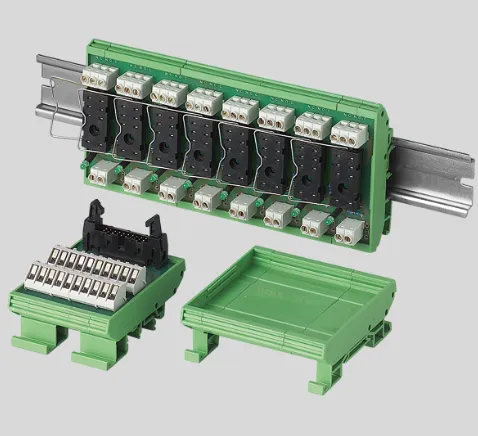
Integrating Heat Sinks PCB Designs
Heat sinks PCB attachments use extruded aluminum fins or pin styles bonded via thermal interface materials like pads or grease for optimal contact. Epoxy or mechanical clips secure sinks without stressing solder joints, vital in vibrating railway settings. Spreader plates distribute load from uneven component heights, ensuring full coverage. For compact signaling boards, low-profile skived fin heatsinks fit within enclosure constraints. Combining with thermal vias funnels board-level heat to the sink, boosting overall efficiency. Surface treatments like anodizing improve emissivity for radiation cooling in still air.
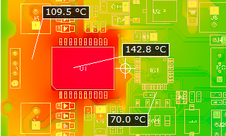
The Role of Thermal Simulation PCB Tools
Thermal simulation PCB software models steady-state and transient behaviors, predicting hotspots before prototyping. Finite element analysis simulates conduction paths, convection coefficients, and radiation factors based on board geometry and materials. Input parameters include power dissipation maps from SPICE simulations and ambient conditions per railway specs. Iterations optimize via placement, trace widths, and sink geometries, reducing physical tests. Validation against measurements refines models for future designs. For railway electronics cooling, simulations account for worst-case scenarios like solar loading on enclosures.
Railway-Specific Challenges and Solutions
Railway signaling PCBs face cyclic thermal loads from diurnal variations and train-induced vibrations, accelerating fatigue in solder and vias. Conformal coatings add insulation, requiring higher dissipation rates to compensate. Enclosure designs incorporate phase-change materials or heat pipes for passive cooling. Active solutions like TECs suit high-power nodes but increase complexity. Hybrid approaches layer board-level tactics with system cooling. Compliance with vibration standards ensures thermal features withstand mechanical stress.
Best Practices for Implementation
Follow IPC-2221 guidelines for trace sizing and spacing to manage heat rise in power sections. IPC-2152 provides charts for current-temperature relationships, preventing excessive trace heating. Layer stackups prioritize inner planes as heat spreaders adjacent to signal layers. Post-assembly infrared thermography verifies dissipation effectiveness. Iterative testing under simulated railway conditions refines designs. Documentation of thermal budgets aids procurement and maintenance teams.
Conclusion
Thermal management in railway signaling PCBs demands a multifaceted approach integrating PCB heat dissipation, thermal vias, heat sinks PCB, and thermal simulation PCB techniques. These strategies ensure reliable railway electronics cooling amid harsh conditions. Electric engineers benefit from structured design principles rooted in conduction enhancement and predictive modeling. Adopting best practices minimizes risks, extends service life, and supports safety imperatives. Future advancements in materials and simulation will further elevate performance. Prioritizing these methods delivers robust boards ready for the rails.
FAQs
Q1: What are the primary methods for PCB heat dissipation in railway signaling systems?
A1: PCB heat dissipation relies on copper planes, thermal vias, and heat sinks to conduct heat away from components. In railway environments, combining these with enclosure ventilation addresses high ambient loads. Engineers select via arrays and thick copper based on power profiles for optimal transfer. This prevents hotspots and maintains signal accuracy.
Q2: How do thermal vias improve cooling in high-power railway PCBs?
A2: Thermal vias provide vertical paths linking surface devices to inner layers, enhancing conduction over solid copper. Arrays under hotspots achieve uniform spreading, crucial for railway electronics cooling. Filling prevents voids, ensuring reliability under vibration. Design per standard guidelines balances density with manufacturability.
Q3: Why is thermal simulation PCB essential for railway applications?
A3: Thermal simulation PCB predicts temperature distributions under operational loads, identifying risks early. It models vias, sinks, and convection for railway-specific scenarios like enclosed heat buildup. Iterations optimize layouts without costly prototypes. Accurate inputs yield designs compliant with reliability needs.
Q4: When should heat sinks PCB be used in signaling boards?
A4: Heat sinks PCB suit applications exceeding 5W dissipation per component, common in power relays. They excel in still-air enclosures typical of railways. Pairing with vias maximizes efficiency. Selection considers footprint, attachment, and vibration resistance for long-term performance.
References
IPC-2221A — Generic Standard on Printed Board Design. IPC, 2003
IPC-2152B — Standard for Determining Current Carrying Capacity in Printed Board Trace. IPC, 2009
IPC-6012E — Qualification and Performance Specification for Rigid Printed Boards. IPC, 2017


