Introduction
Thin printed circuit boards play a pivotal role in modern medical devices, where space constraints and miniaturization demands drive innovation. These boards, often required in applications like wearable monitors, implantable devices, and portable diagnostics, must deliver high performance while maintaining unwavering reliability. Engineers face unique challenges in medical device PCB design, balancing compactness with the need for long-term functionality in harsh biological environments. Reliability thin PCB medical applications becomes paramount, as any failure can have life-critical consequences. This article explores the engineering principles, design strategies, and best practices to ensure thin PCBs meet the stringent demands of healthcare technology. By adhering to established standards, designers can achieve robust solutions that support patient safety and device efficacy.
Understanding Thin PCBs in Medical Applications
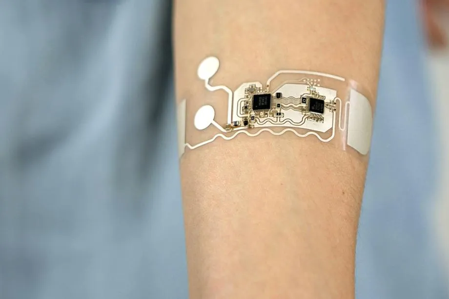
Thin PCBs refer to rigid or flexible boards with reduced thickness to fit into compact medical devices, enabling closer integration with sensors and actuators. In thin PCB medical applications, such boards appear in endoscopes, insulin pumps, and cardiac rhythm management systems, where bulkier alternatives would compromise usability. The push for miniaturization stems from the need for less invasive procedures and improved patient comfort, but it introduces risks like mechanical fragility and thermal vulnerabilities. Engineers must consider how reduced material volume affects electrical performance and structural integrity under operational stresses. Why does this matter? In critical healthcare settings, these boards must withstand repeated use, bodily fluids, and sterilization processes without degradation.
The relevance intensifies with the rise of personalized medicine, where devices demand high-density interconnects in limited spaces. Thin designs facilitate high-speed signal transmission essential for real-time data processing in diagnostics. However, achieving reliability requires meticulous material selection and process controls from the outset. Medical device PCB design thus emphasizes prevention of common pitfalls like delamination or shorts. Ultimately, thin PCBs bridge the gap between advanced functionality and practical deployment in life-sustaining equipment.
Key Technical Principles for Reliability
Reliability in thin PCBs hinges on managing warpage, a primary concern due to asymmetric thermal expansion in thinner constructions. During fabrication and assembly, temperature gradients cause copper foils and substrates to expand differently, leading to board curvature that misaligns components. Engineers mitigate this through symmetric stackups, where core and prepreg layers balance coefficients of thermal expansion. Signal integrity also demands attention, as thinner dielectrics reduce impedance control margins, potentially causing crosstalk in high-frequency medical signals. Adherence to IPC-6012 specifications ensures qualification tests verify performance under thermal cycling and mechanical shock.
Material properties dominate reliability thin PCB medical scenarios. Substrates must exhibit low moisture absorption to prevent popcorn effects during reflow soldering. Vias and traces require precise plating to endure flexing in semi-rigid designs common in wearables. Electrical testing confirms continuity and insulation resistance post-fabrication. These principles form the foundation for boards that operate flawlessly in vivo environments.
Another critical aspect involves environmental resilience. Thin boards face accelerated degradation from humidity and chemicals, necessitating robust surface finishes like ENIG for corrosion resistance. Finite element analysis simulates stress distributions, guiding layout optimizations. By integrating these mechanisms, designers achieve predicted lifecycles matching device requirements.
Design Challenges: Sterilization and Biocompatibility
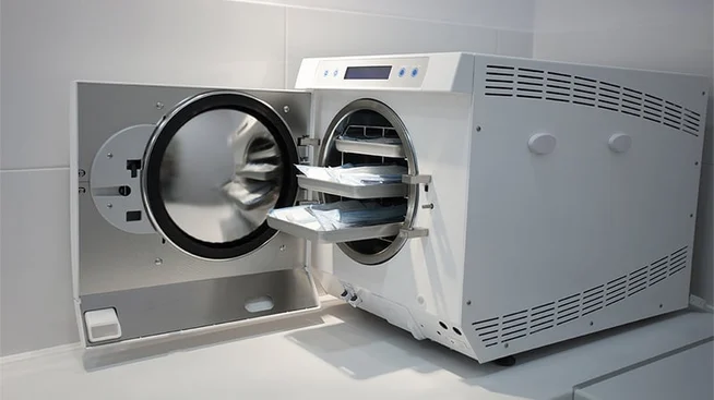
Sterilization thin PCB processes pose significant hurdles, as methods like ethylene oxide, gamma radiation, and autoclaving stress materials differently. Gamma rays can embrittle polymers, while steam autoclaves induce hydrolysis in laminates. Engineers select resins with high glass transition temperatures and radiation-stable formulations to maintain interlayer adhesion. Pre-sterilization qualification involves accelerated aging tests to predict long-term integrity. Compatibility ensures no residue leaching that could contaminate sterile fields.
Biocompatible thin PCB requirements extend to material outgassing and cytotoxicity. Substrates and finishes must pass biological evaluation to avoid inflammatory responses in implants. Low-halogen compositions reduce toxic emissions during high-heat sterilization. Design teams incorporate barriers like conformal coatings tuned for medical grades, preserving electrical properties while enhancing barrier functions. These considerations align with ISO 13485 quality management systems, embedding risk assessments into the design phase.
Handling thin boards amplifies contamination risks, demanding cleanroom protocols beyond standard assembly. Particle-induced shorts become more likely with proximity of traces. Ultrasonic cleaning verifies ionic residues stay below thresholds. Troubleshooting focuses on root-cause analysis, such as via cracking from mishandling, resolved via carrier panels during processing.
Best Practices in Medical Device PCB Design
Effective medical device PCB design for thin boards starts with stackup planning to minimize warpage. Balance copper weights across layers and incorporate blind vias for density without full-thickness penetration. Controlled impedance modeling verifies trace geometries suit signal speeds in diagnostics. Larger pad sizes accommodate handling tolerances, reducing placement defects. Fabrication partners should confirm capabilities via design for manufacturability reviews.
Assembly processes demand specialized fixtures to prevent flexing during solder paste application and reflow. Low-temperature solders preserve thin board integrity, while nitrogen atmospheres curb oxidation. Post-assembly, X-ray inspection detects voids invisible externally. Reliability thin PCB medical validation includes thermal shock and vibration per application profiles.
For sterilization thin PCB resilience, qualify assemblies under repeated cycles mimicking clinical use. Select coatings with proven permeability resistance to gases. Biocompatible thin PCB validation involves extractables testing early in development. Documentation traces materials to certificates, supporting regulatory submissions. These practices ensure compliance and field performance.
Advanced Considerations: Testing and Qualification
Qualification testing verifies thin PCBs endure operational extremes. Thermal cycling per IPC-6012 exposes boards to -40°C to 125°C swings, checking for microcracks. Humidity bias simulates implant conditions, monitoring leakage currents. Mechanical bend tests assess flex limits for hybrid rigid-flex designs. Data from these informs design iterations, closing the loop on reliability.
In troubleshooting, warpage often traces to bake-out omissions pre-lamination. Solution: Implement moisture control per JEDEC guidelines, though adapted for medical. Signal loss in thin dielectrics resolves via ground plane stitching. Field failures, rare with rigorous processes, prompt failure mode analysis. Engineers log lessons for future designs.
Ensuring Long-Term Performance in Critical Applications
Integration with device enclosures demands thin PCB conformal protection against biofluids. Silicone or parylene types provide hermetic seals without compromising flexibility. EMI shielding via grounded pours maintains compliance with IEC 60601 electromagnetic requirements. Battery interfaces require careful routing to avoid shorts in compact layouts.
Sustainability enters via lead-free processes, aligning with medical trends. Recyclable materials support end-of-life directives without biocompatibility trade-offs. Procurement specifies Class 3 conformance, ensuring supplier alignment.
Conclusion
Thin PCBs revolutionize medical devices by enabling compact, high-performance solutions critical for patient care. Mastering reliability involves holistic design addressing warpage, sterilization, and biocompatibility challenges. Best practices grounded in standards like IPC-6012 and ISO 13485 deliver boards that perform under scrutiny. Engineers prioritizing these elements ensure devices meet clinical demands, fostering trust in healthcare technology. As applications evolve, ongoing qualification solidifies thin PCB medical applications as reliable cornerstones.
FAQs
Q1: What are the main challenges in thin PCB medical applications?
A1: Thin PCB medical applications face issues like warpage from thermal stresses, fragility during handling, and signal integrity in dense layouts. Sterilization processes can degrade materials, while biocompatibility demands low-toxicity selections. Engineers counter these with symmetric designs, specialized testing, and qualified substrates, ensuring reliability in wearables and implants. Adhering to medical device PCB design principles minimizes risks effectively.
Q2: How does sterilization impact thin PCB reliability?
A2: Sterilization thin PCB methods such as gamma or autoclave expose boards to radiation or moisture, risking delamination or embrittlement. Materials must resist hydrolysis and maintain adhesion post-process. Qualification involves cycle testing to verify electrical stability. Proper preparation, like thorough drying, preserves reliability thin PCB medical performance over multiple uses.
Q3: What makes a thin PCB biocompatible for medical devices?
A3: Biocompatible thin PCB selection focuses on non-cytotoxic laminates and finishes with minimal extractables. Testing evaluates skin irritation and sensitization per standards. Coatings enhance barriers without altering dielectrics. In medical device PCB design, traceability from raw materials ensures compliance, supporting safe implantation or external contact.
Q4: Why prioritize IPC Class 3 for reliability thin PCB medical?
A4: IPC Class 3 imposes strict tolerances on annular rings, plating, and cleanliness for high-reliability environments. It suits critical medical uses by mandating zero breakout and superior conductor definition. This level prevents intermittent failures in thin constructions, aligning with ISO 13485 quality systems for consistent outcomes.
References
IPC-6012F — Qualification and Performance Specification for Rigid Printed Boards. IPC, 2023
ISO 13485:2016 — Medical devices — Quality management systems — Requirements for regulatory purposes. ISO, 2016
IEC 60601-1:2005+A1:2012+A2:2020 — Medical electrical equipment — Part 1: General requirements for basic safety and essential performance. IEC, 2020


