Introduction
Flexible thin PCBs represent a significant advancement in electronics, enabling designs that conform to irregular shapes and withstand repeated bending. These boards, often essential in modern devices, combine thin profiles with high flexibility to support applications demanding compactness and durability. Engineers increasingly rely on flexible thin PCBs for innovations like wearable technology and curved displays, where traditional rigid boards fall short. This article explores the fundamentals, materials, design considerations, and reliability factors of flexible thin PCBs, providing factory-driven insights aligned with industry standards. Understanding these elements ensures optimal performance in demanding environments. Key aspects include the bending radius thin PCB capabilities and materials for flexible thin PCB construction.
What Are Flexible Thin PCBs and Why Do They Matter?
Flexible thin PCBs consist of thin layers of conductive traces embedded in flexible substrates, allowing them to bend, twist, and fold without compromising functionality. Unlike rigid printed boards, these use pliable materials that maintain electrical integrity under mechanical stress, making them ideal for space-constrained assemblies. In the PCB manufacturing process, flexible thin PCBs emerge from specialized lamination techniques that bond copper foils to substrates like polyimide films. Their relevance grows in industries requiring lightweight, compact solutions, such as consumer electronics and medical devices. Factory production emphasizes precise control over thickness to achieve the desired flexibility while meeting performance specifications. Adopting flexible thin PCBs reduces assembly complexity and enhances product reliability in dynamic applications.
Materials for Flexible Thin PCB Construction
Selecting appropriate materials forms the foundation of reliable flexible thin PCB performance. Polyimide substrates dominate due to their excellent thermal stability, chemical resistance, and flexibility, supporting operations in harsh environments. Polyester offers a cost-effective alternative for less demanding static applications, though it has lower temperature tolerance. Adhesive-less laminates provide superior bend endurance compared to adhesive-based ones, as they minimize delamination risks during flexing. Copper foil type also influences material properties, with rolled annealed copper preferred for its ductility in high-flex zones. Manufacturers must align material choices with application needs to ensure long-term integrity.
Coverlay films protect traces and contribute to overall flexibility, often applied post-etching in production. The combination of substrate, copper, and coverlay determines the board's ability to handle repeated cycles without failure. Factory insights highlight the importance of consistent material thickness control during lamination to avoid warpage.
Understanding Bending Radius in Thin PCBs
The bending radius thin PCB specification defines the minimum curvature a board can endure without damage, critical for dynamic applications. Factors like substrate thickness, copper weight, and layer count directly impact this radius, with thinner constructions allowing tighter bends. In design, engineers calculate the bend radius based on static or dynamic flex requirements, where dynamic use demands larger radii to prevent fatigue. IPC-2223 provides guidelines for designing flexible printed boards, emphasizing bend area layouts that distribute stress evenly. Avoiding sharp bends and incorporating strain relief features enhances durability. Factory testing verifies these parameters through controlled flex cycles.
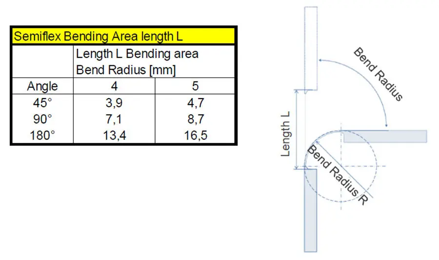
Multi-layer flexible thin PCBs require staggered trace routing in bend zones to reduce stress concentrations. Manufacturers recommend wider traces and teardrops at vias in flex areas for better reliability. Proper bend radius management prevents cracks in copper or substrate delamination over time.
Manufacturing Process for Flexible Thin PCBs
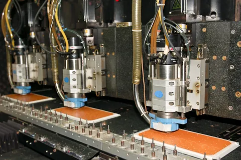
Producing flexible thin PCBs involves adapted processes to handle delicate materials, starting with substrate preparation and copper lamination. Photolithography etches precise traces, followed by coverlay application for insulation. Lamination occurs under controlled pressure and temperature to bond layers without voids. In rigid-flex hybrids, rigid sections integrate seamlessly with flex tails. Best practices include using adhesive-less materials for high-flex regions and precise registration for multi-layer alignment. Factories employ cleanroom environments to minimize contamination on thin substrates.
Post-processing steps like outline routing demand specialized tooling to avoid tearing. IPC-6013 outlines qualification requirements for flexible printed boards, ensuring performance consistency. Engineers benefit from collaborating early with manufacturers to refine stackups.
Ensuring Reliability of Flexible Thin PCBs
Reliability of flexible thin PCBs hinges on rigorous testing protocols that simulate real-world stresses. Bend cycle tests evaluate endurance by repeatedly flexing the board to specified radii, revealing fatigue limits. Thermal cycling assesses material stability under temperature swings, while humidity exposure checks for degradation. Peel strength tests verify adhesion between layers, crucial for dynamic applications. IPC-6013 specifies performance criteria, including electrical and mechanical qualifications. Factory-driven validation confirms boards meet these benchmarks before shipment.
Vibration and shock testing further prove robustness in automotive or aerospace uses. Design mitigations like stiffeners in non-flex areas bolster overall reliability. Monitoring trace integrity post-flexing ensures signal performance remains uncompromised.
Applications: Thin PCBs for Flexible Displays and Beyond
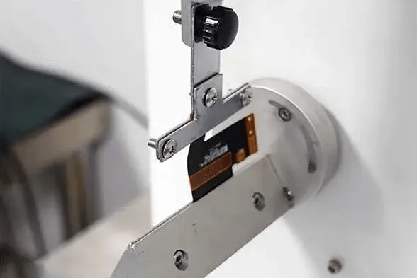
Thin PCB for flexible displays exemplifies the technology's transformative role, enabling foldable screens in smartphones and tablets. These boards integrate seamlessly into curved or rollable panels, supporting high-density interconnects for pixel control. In wearables, flexible thin PCBs conform to body contours, enhancing comfort and functionality. Medical devices use them for implantable sensors that navigate tight spaces. Automotive applications include dynamic tail lights and sensor arrays. The versatility stems from their lightweight nature and adaptability.
Consumer electronics benefit from reduced weight and volume, improving battery life. Emerging uses in robotics demand high reliability of flexible thin PCBs under continuous motion.
Best Practices for Designing and Implementing Flexible Thin PCBs
Adhere to standards like IPC-2223 during layout to optimize bend zones and trace routing. Define flex and rigid areas clearly in the stackup, avoiding vias in high-stress regions. Incorporate fillets on pads and rounded bends to distribute strain. Select materials matching thermal and mechanical demands, prioritizing adhesive-less polyimide for dynamic flex. Simulate flex performance using finite element analysis for early issue detection. Collaborate with manufacturers for design rule checks.
Use tear stops at bend edges and guards around cutouts. Stiffeners reinforce connector areas without impeding flexibility. These practices align with factory capabilities for yield optimization.
Conclusion
Flexible thin PCBs drive innovation in electronics by offering unmatched adaptability and compactness. Key considerations like materials for flexible thin PCB, bending radius thin PCB limits, and reliability of flexible thin PCBs ensure successful implementations. Factory-aligned standards such as IPC-6013 and IPC-2223 guide design and production for consistent quality. Engineers can leverage these insights to push boundaries in flexible displays and beyond. Prioritizing best practices minimizes risks and maximizes performance in real-world deployments.
FAQs
Q1: What materials are best for flexible thin PCB applications?
A1: Polyimide substrates excel in flexible thin PCB due to high thermal resistance and flexibility, ideal for dynamic bending. Adhesive-less versions enhance reliability by reducing delamination risks. Polyester suits static uses with lower costs. Factory selection depends on temperature, flex cycles, and environmental exposure for optimal performance.
Q2: How does bending radius affect thin PCB design?
A2: Bending radius thin PCB determines safe curvature limits, influenced by thickness and copper type. Tighter radii suit thin constructions but risk fatigue in dynamic apps. Design per IPC-2223 guidelines with strain relief ensures durability. Testing verifies limits for specific stackups.
Q3: What tests ensure reliability of flexible thin PCBs?
A3: Reliability of flexible thin PCBs involves bend cycling, thermal shock, and peel adhesion tests per IPC-6013. These simulate operational stresses to detect failures early. Factory protocols confirm electrical continuity post-flexing. Vibration and humidity tests add robustness for harsh environments.
Q4: Why use thin PCBs for flexible displays?
A4: Thin PCB for flexible displays enable folding and curving without bulk, supporting high-resolution interconnects. Their pliability integrates into slim profiles for foldables. Materials withstand repeated flexing, maintaining signal integrity. This drives compact, durable consumer tech innovations.
References
IPC-6013DS with Amendment 1 — Qualification and Performance Specification for Flexible and Rigid-Flex Printed Boards. IPC, 2020
IPC-2223C — Sectional Design Standard for Flexible/Rigid-Flexible Printed Boards. IPC, 2019


