Introduction
In the competitive landscape of PCB manufacturing, achieving high PCB panelization efficiency is essential for reducing costs and improving turnaround times. Engineers often focus on individual board designs, yet the maximum PCB size profoundly influences how effectively panels are utilized during production. Larger boards occupy more space, potentially leading to fewer units per panel and increased material waste, which directly affects PCB manufacturing yield. By understanding this relationship, designers can implement panel size optimization strategies that enhance cost-effective PCB design. This article delves into the mechanics of panel utilization, offering factory-driven insights aligned with industry standards to help electric engineers maximize boards per panel without compromising quality.
Panelization transforms single PCBs into arrays on larger sheets, streamlining fabrication and assembly processes. However, suboptimal sizing leads to inefficiencies that compound across high-volume runs. Key factors like board dimensions, spacing requirements, and depanelization methods determine overall yield. Optimizing these elements ensures better resource use and aligns with manufacturing realities.
What Is PCB Panelization and Why Does Panel Utilization Matter?
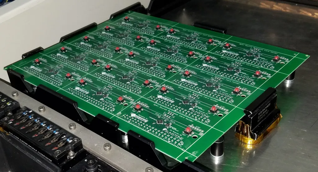
PCB panelization involves arranging multiple identical or mixed individual circuit boards onto a single production panel to facilitate batch processing in fabrication and assembly. This approach minimizes handling time, reduces setup costs per board, and improves throughput in automated lines. Panel utilization refers to the ratio of active board area to the total panel area, expressed as a percentage, where higher values indicate better efficiency and lower waste.
Poor panel utilization arises when maximum PCB size exceeds optimal thresholds relative to standard panel formats, resulting in unused margins or incomplete arrays. This inefficiency elevates per-board costs, as fixed expenses like etching and plating are spread across fewer units. For electric engineers, recognizing this impact is crucial during the design phase to support PCB manufacturing yield targets. Industry practices emphasize balancing board size with panel constraints to achieve sustainable production economics.
In high-reliability applications, panelization also aids in maintaining consistent process controls, such as temperature uniformity during reflow soldering. Suboptimal layouts can introduce variations in thermal profiles or mechanical stresses across the array. Thus, panel size optimization becomes a cornerstone of cost-effective PCB design, directly tying design choices to operational outcomes.
Technical Principles Behind Maximum PCB Size and Panel Utilization
The core principle governing panel utilization is geometric nesting: fitting as many PCBs as possible within fixed panel boundaries while accounting for mandatory margins, spacing, and fiducials. Maximum PCB size dictates the base unit area, where larger dimensions reduce the feasible count per panel due to simple division constraints. For rectangular boards, engineers calculate potential arrays by dividing panel dimensions by combined board and inter-board spacing, often revealing that oversized designs yield only one or two units per panel.
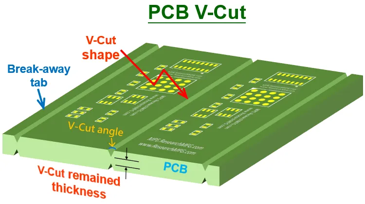
Depanelization methods further constrain layouts. V-scoring requires precise linear separations with minimal spacing between boards, ideal for uniform arrays but sensitive to size mismatches. Tab routing, conversely, demands wider tabs and breakout zones, increasing waste around larger PCBs. These choices amplify the effect of maximum PCB size, as oversized boards exacerbate edge losses in either method.
Material properties and process tolerances also interplay. Panels must include border rails for handling and tooling holes per manufacturing norms, typically consuming 10 to 20 percent of the area regardless of board size. Larger PCBs amplify this proportional waste, lowering overall utilization. Compliance with IPC-2221 generic design standards ensures layouts account for these factors, promoting manufacturability from the outset.
Warpage risks heighten with panel scale, particularly for thick or high-layer-count boards. Oversized panels with large PCBs experience greater thermal expansion differentials during lamination or baking, potentially violating flatness specs in IPC-6012E qualification requirements. Engineers mitigate this by selecting panel sizes that distribute stresses evenly, preserving PCB manufacturing yield.
Irregular board shapes compound challenges, as non-rectangular outlines demand custom nesting algorithms to minimize gaps. Maximum PCB size in these cases refers to the bounding rectangle, which inefficiently represents the actual area. Optimization involves rotating orientations or mirroring boards to tessellate effectively, a practice rooted in factory-driven efficiency metrics.
Factors Influencing Panel Utilization Efficiency
Several interrelated factors determine how maximum PCB size impacts utilization. Standard panel formats, such as those around 18 by 24 inches, set the canvas, with usable areas reduced by perimeter clearances for fixturing and transport. Boards approaching half the panel length often limit arrays to four or fewer, slashing efficiency compared to smaller designs fitting dozens.
Spacing requirements vary by process step. Fabrication needs fiducials and alignment marks outside board outlines, while assembly demands zones for pick-and-place stencils. Larger PCBs encroach on these, forcing wider gaps or single-board panels, which undermine PCB panelization efficiency. Engineers must model these in design reviews to forecast yield.
Layer count and thickness influence feasibility. Multilayer boards with large dimensions strain inner layer registration during lamination, increasing scrap rates. Panel size optimization here involves selecting formats that align with press capacities, ensuring uniform pressure distribution.
Component placement near edges affects routing paths for depanelization. Oversized boards with edge-mounted parts require extended tabs or scores, inflating margins. This design-layout interplay underscores why maximum PCB size must integrate with overall DFM considerations.
Practical Solutions and Best Practices for Maximizing Boards per Panel
To counter the limitations of large PCB sizes, start with panel size optimization during schematic-to-layout transition(see our guide on PCB size optimization best practices). Select standard panel dimensions that are multiples of the PCB footprint, allowing tight arrays with minimal rotation trials. For instance, rectangular boards benefit from orthogonal or 90-degree rotations to fill voids, boosting utilization by 10 to 30 percent in typical scenarios.
Incorporate factory-aligned margins: allocate 0.5-inch borders for handling and 0.125-inch tabs for routing, scaling with board size. Place fiducials in corners, away from active areas, to support optical alignment without eroding usable space. These practices, drawn from IPC-A-600 acceptability criteria, ensure panels process reliably.
Employ array generators in design environments to simulate layouts, prioritizing high-utilization configurations. Mix board orientations judiciously, especially for aspect ratios near 1:1, to nest efficiently. Test virtual panels against real-world constraints like stencil tolerances for cost-effective PCB design.
For oversized prototypes, consider partial panels or singles initially, scaling to full arrays in production. Collaborate with manufacturing on depanelization preferences early, as V-scoring suits high-density small boards while routing handles complex large ones. This proactive approach elevates PCB manufacturing yield.
Monitor utilization targets above 70 percent as a benchmark, adjusting designs iteratively. Document panel specs in fabrication drawings, including breakaway rules, to streamline quoting and production.
Real-World Insights: Balancing Size and Efficiency
Consider a mid-sized consumer device PCB versus an industrial control board. The former, compact at under 100 square inches, panels into 20-plus units on standard formats, yielding high efficiency. The latter, spanning larger areas, might fit only four to six, necessitating custom panels that inflate costs unless optimized.
Troubleshooting low utilization often reveals overlooked margins or fiducial conflicts. Engineers audit layouts against process flows, resizing or reshaping where feasible without functional tradeoffs. Such factory-driven adjustments align with ISO 9001 quality systems, fostering repeatable high-yield outcomes. For deeper coverage of V-scoring techniques, refer to our PCB panelization V-scoring guide.
Conclusion
Maximum PCB size fundamentally shapes PCB panelization efficiency, dictating boards per panel and overall manufacturing economics. By prioritizing geometric optimization, standard-compliant margins, and depanelization compatibility, engineers unlock substantial gains in yield and cost savings. Panel size optimization emerges as a pivotal DFM lever, transforming potential waste into productive arrays. Adopting these structured practices empowers cost-effective PCB design, ensuring robust production scalability for electric engineering projects. Learn more about standard panel dimensions in our article on standard PCB dimensions and cost efficiency.
FAQs
Q1: What is PCB panelization efficiency, and how does it relate to maximum PCB size?
A1: PCB panelization efficiency measures the usable board area versus total panel area, directly impacted by maximum PCB size. Larger boards reduce the number that fit, lowering the ratio and increasing waste. Optimizing layouts with rotations and minimal spacing counters this, aligning with manufacturing standards for better yield. Factory insights emphasize early size checks to sustain high efficiency.
Q2: How can engineers maximize boards per panel in production?
A2: Maximizing boards per panel involves selecting panel formats matching PCB dimensions, incorporating precise spacing, and using efficient nesting. Account for borders, fiducials, and depanelization to avoid waste. Simulate arrays to test rotations and orientations, targeting high utilization. This approach enhances PCB manufacturing yield without altering core designs.
Q3: Why is panel size optimization key to cost-effective PCB design?
A3: Panel size optimization minimizes material use and setup times by fitting more boards, spreading fixed costs thinner. Large PCB sizes demand tailored panels, raising expenses, while optimized ones leverage standard processes. Compliance with design standards ensures manufacturability, reducing iterations and supporting scalable production economics.
Q4: What role do depanelization methods play in PCB panelization efficiency?
A4: Depanelization methods like V-scoring or tab routing dictate inter-board spacing, influencing how many large PCBs fit per panel. V-scoring enables zero-gap arrays for efficiency, while routing needs wider tabs for bigger boards. Choosing based on size optimizes utilization, preserving integrity post-separation.
References
IPC-6012E — Qualification and Performance Specification for Rigid Printed Boards. IPC, 2017
IPC-A-600K — Acceptability of Printed Boards. IPC, 2020
IPC-2221 — Generic Standard on Printed Board Design. IPC, 2012


