Introduction
Wearable electronics continue to push the boundaries of traditional rigid PCB designs, demanding materials and structures that conform to the human body while maintaining electrical reliability. Flexible polyimide PCBs emerge as a cornerstone solution, offering exceptional bendability combined with thermal and mechanical stability essential for devices like smartwatches, fitness trackers, and health monitors. Polyimide, a high-performance polymer, serves as the substrate of choice in these applications due to its ability to endure repeated flexing without degradation. Engineers designing for wearables must grasp the intricacies of flexible polyimide PCB design rules to optimize performance and longevity. This article delves into the principles, calculations, and best practices that enable innovative wearable designs. By adhering to established guidelines, designers can mitigate risks such as trace cracking or delamination in dynamic environments.
What Are Flexible Polyimide PCBs and Why Do They Matter for Wearables?
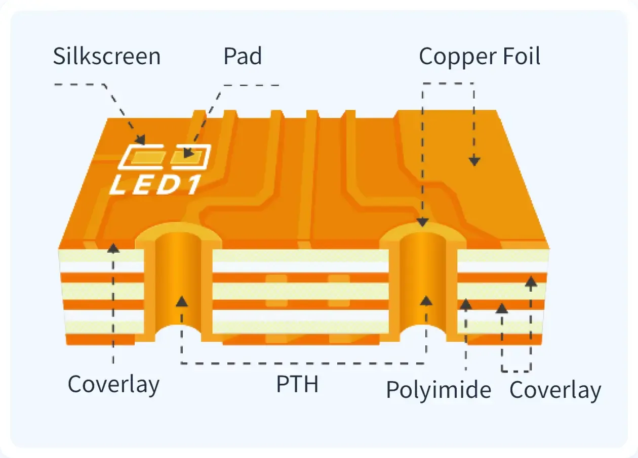
Flexible polyimide PCBs consist of thin polyimide films laminated with copper conductors, often in adhesiveless constructions to enhance bend performance. Polyimide provides superior flexibility, chemical resistance, and thermal stability compared to alternatives like polyester, making it ideal for wearable electronics PCB materials. In wearables, where space constraints and user movement impose constant mechanical stress, these PCBs allow circuits to twist, fold, and stretch without failure. The material's low coefficient of thermal expansion minimizes warpage during assembly processes involving soldering or reflow. Designers select polyimide for its balance of electrical properties, such as a dielectric constant around 3.2 to 3.5, ensuring signal integrity in compact layouts. Ultimately, flexible polyimide PCBs enable slimmer profiles and lighter weights, critical for user comfort in prolonged wear.
The relevance intensifies in wearables, where rigid boards limit form factors and increase bulk. Polyimide substrates support dynamic flexing required for wristbands or head-mounted devices, accommodating millions of bend cycles in high-reliability applications. Standards like IPC-2223 outline classifications for single-sided, double-sided, and multilayer flex boards, guiding material selection for these uses. Engineers must consider polyimide's robustness against environmental factors, including moisture and vibration common in fitness tracking. This material choice directly impacts device reliability, battery life, and sensor accuracy in real-world scenarios. As wearable tech evolves toward biomedical implants and augmented reality glasses, polyimide's proven track record solidifies its position.
Core Technical Principles of Flexible Polyimide PCB Design Rules
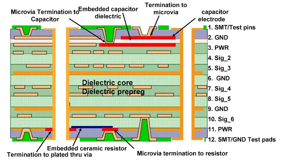
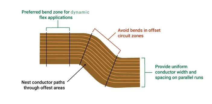
Flexible polyimide PCB design rules revolve around material properties, conductor layout, and mechanical constraints to prevent fatigue failure. Polyimide films, typically 25 to 100 micrometers thick, form the dielectric core, paired with rolled annealed copper for dynamic applications to allow greater elongation without cracking. IPC-2223 specifies conductor routing perpendicular to the bend axis, staggering traces between layers to avoid stiffening effects, and prohibiting vias in flex zones. Coverlay materials, often polyimide-based, protect traces while maintaining flexibility, with access holes requiring minimum overlaps and relief cuts at corners. Ground planes in bend areas use crosshatch patterns rather than solid fills to preserve bendability. These rules ensure electrical continuity under stress, vital for signal-sensitive wearables.
Layer count influences design complexity, with single-sided types suiting simple sensor interfaces and multilayers handling power distribution. Adhesiveless builds, where copper integrates directly onto polyimide, reduce thickness and improve peel strength over adhesive-based laminates. Trace widths widen in static regions but narrow in dynamic bends, with teardrop transitions to pads mitigating stress concentrations. Stiffeners, such as thin polyimide or FR-4, reinforce component mounting areas without compromising overall flex. Engineers simulate neutral bend axes, positioning critical traces centrally to balance compression and tension. Compliance with IPC-6013 during qualification verifies these designs through bend and thermal cycling tests.
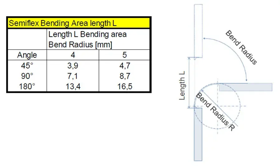
Polyimide PCB Bend Radius Calculation: Engineering the Limits
Polyimide PCB bend radius calculation determines the minimum curvature a flex section can endure without damage, calculated as R = T × N, where T is total flex thickness and N is the application-specific ratio. Static bending, occurring fewer than 100 times during installation, uses lower ratios like 6:1 for single-layer or 12:1 for double-layer per IPC-2223 guidelines. Dynamic applications in wearables demand higher factors, such as 100:1 for single-layer, escalating to 150:1 or 200:1 for multilayers to accommodate repeated cycles. Thickness T includes copper, polyimide substrate, and coverlay, typically ranging from 0.043 mm to 0.205 mm in common stackups. For a 0.15 mm double-layer dynamic flex, static radius measures 1.8 mm while dynamic reaches 22.5 mm, factoring inner surface measurements and safety margins of 20 to 30 percent. Temperature variations stiffen polyimide at low ends, necessitating prototype validation.
Typical ratios by layer count:
- Single layer — Static 6:1; Dynamic 100:1
- Double layer — Static 12:1; Dynamic 150:1
- Multilayer — Static 24:1; Dynamic 200:1
Designers apply these in CAD tools by defining bend zones early, ensuring tear stops and gradual fillets precede sharp transitions. Rolled annealed copper's ductility supports tighter radii versus electrodeposited types, crucial for polyimide's thin profiles. Multi-axis bending in wearables compounds stress, prompting unbonded "bookbinder" constructions for multilayers. Post-calculation, finite element analysis predicts strain distribution across the polyimide substrate. Avoiding discontinuities like sharp corners or dense via fields preserves the calculated limits. This structured approach aligns flexible polyimide PCB design rules with manufacturing feasibility.
Practical Best Practices for Wearable Electronics Implementations
Implement flexible polyimide PCB design rules by prioritizing adhesiveless laminates for wearables, minimizing moisture absorption and enabling thinner profiles under 0.1 mm. Route high-speed signals away from bend areas, using perpendicular orientations and crosshatch planes to distribute stress evenly across polyimide layers. Integrate stiffeners selectively, extending 0.5 mm beyond footprints with pressure-sensitive adhesives, to support SMD components without inducing rigidity. Transition zones in rigid-flex hybrids stagger layer ends 1.25 mm from edges, incorporating strain relief fillets for seamless rigid-to-flex handoff. Prototype testing per IPC-TM-650 methods, including cyclic bending and thermal shock, validates polyimide PCB bend radius calculations in simulated wear conditions. Fabricate with controlled tolerances, such as 8 mil drill-to-copper distances, to enhance alignment in dynamic assemblies.
For wearable electronics PCB materials, select polyimide grades with proven thermal stability to withstand body heat and sweat exposure. Avoid 90-degree bends by filleting corners with radii exceeding 0.75 mm, and insert relief holes in coverlay for flexibility. Power and ground distribution employs split wide traces in bends, preventing "I-beam" effects that crack polyimide interfaces. Environmental sealing via conformal coatings preserves long-term integrity without sacrificing flex. Collaborate with fabricators early to confirm RA copper availability and coverlay thicknesses matched to copper weights. These practices extend device lifespan beyond 200,000 cycles in fitness trackers.
Common Challenges and Troubleshooting in Dynamic Flex Designs
Challenges arise from underestimating dynamic stress in wearables, leading to copper fatigue or polyimide delamination after prolonged use. Symptoms include resistance spikes or intermittent opens, traced to trace cracking at bend edges violating polyimide PCB bend radius calculation limits. Mitigate by upscaling radii 20 percent beyond minima and validating via dynamic bend tests simulating user motions. Multilayer designs risk interlayer slippage if adhesives degrade; opt for adhesiveless builds and monitor peel strength per IPC-TM-650. Thermal mismatches between polyimide and rigid sections cause warpage; balance CTE through symmetric stackups. Troubleshooting involves micro-sectioning failed prototypes to inspect neutral axis shifts, adjusting stiffener overlaps accordingly.
Vibration in activity trackers amplifies fatigue; incorporate damping via patterned grounds. Signal integrity degrades in high-frequency bends due to impedance variations; use TDR testing early. Overly thin polyimide risks puncture; pair with robust coverlays exceeding 25 micrometers. Iterative DFMA reviews catch routing violations before production. These insights, rooted in IPC-6013 acceptance criteria, ensure class 3 reliability for medical wearables.
Conclusion
Flexible polyimide PCBs redefine wearable designs through their unmatched blend of flexibility, durability, and electrical performance. Mastering flexible polyimide PCB design rules, including precise polyimide PCB bend radius calculations, empowers engineers to create resilient circuits for dynamic applications. Adhering to standards like IPC-2223 guarantees manufacturability and field reliability, from fitness bands to smart textiles. Polyimide stands out among wearable electronics PCB materials for its thermal resilience and lightweight nature, enabling form factors impossible with rigid alternatives. Future innovations will leverage multilayer adhesiveless builds for even tighter integrations. Prioritize these principles to bend the rules effectively without breaking them.
FAQs
Q1: What are the key flexible polyimide PCB design rules for wearables?
A1: Flexible polyimide PCB design rules emphasize perpendicular trace routing to bends, staggered layering, and no vias in flex zones per IPC-2223. Use adhesiveless polyimide with rolled annealed copper for dynamic flexing, and apply crosshatch planes to maintain flexibility. Coverlay overlaps ensure protection, while stiffeners support components selectively. These rules prevent cracking and delamination in body-conforming devices, optimizing for repeated motion.
Q2: How do you perform polyimide PCB bend radius calculation?
A2: Polyimide PCB bend radius calculation uses R = T × N, where T is total thickness and N derives from static (6–24:1) or dynamic (100–200:1) ratios based on layers. For a single-layer static bend at 0.1 mm thick, R equals 0.6 mm; dynamic scales to 10 mm. Add safety margins and prototype test to account for temperature effects on polyimide stiffness. This ensures wearable circuits withstand user-induced stresses reliably.
Q3: Why choose polyimide as a wearable electronics PCB material?
A3: Polyimide excels in wearable electronics PCB materials due to its flexibility, thermal stability up to high temperatures, and low CTE for assembly compatibility. It supports thin, lightweight designs conforming to body contours while resisting chemicals and moisture. Compared to polyester, polyimide handles dynamic bending better, ideal for health monitors. Standards like IPC-4202 qualify its dielectric properties for reliable performance.
Q4: What tests verify flexible polyimide PCB reliability?
A4: Tests per IPC-6013 and IPC-TM-650 include static/dynamic bend cycling, thermal shock, and peel strength to confirm polyimide integrity. Dynamic tests simulate wearable motions over thousands of cycles, checking for trace cracks or delamination. Electrical continuity and impedance hold under flex stress. Class 3 criteria demand zero defects for high-reliability wearables.
References
IPC-2223 — Sectional Design Standard for Flexible Printed Boards. IPC
IPC-6013 — Qualification and Performance Specification for Flexible and Rigid-Flex Printed Boards. IPC
IPC-TM-650 — Test Methods Manual. IPC