Introduction
Halogen-free PCBs have become essential in modern electronics manufacturing due to increasing regulatory pressures and customer demands for sustainable products. These boards eliminate halogens such as chlorine and bromine from their base materials, preventing the release of toxic gases during combustion or disposal. While offering environmental benefits, halogen-free PCBs often carry higher production costs compared to traditional halogenated options, prompting engineers to seek ways for reducing halogen-free PCB cost. Factory-driven approaches focus on material choices, design tweaks, and process controls to deliver affordable halogen-free PCBs without sacrificing quality. This article provides practical strategies drawn from manufacturing insights, emphasizing compliance with established standards. By implementing these solutions, production teams can achieve cost-effective outcomes tailored to high-volume needs.
What Are Halogen-Free PCBs and Why Do They Matter?
Halogen-free PCBs use laminates and prepregs with less than 900 parts per million of chlorine or bromine individually, and less than 1500 parts per million total for these elements combined. This definition aligns with specifications in IPC-4101B for base materials used in rigid and multilayer printed boards. Traditional PCBs rely on brominated flame retardants like TBBPA for fire resistance, but these release harmful dioxins and hydrogen bromide when burned. Halogen-free alternatives employ phosphorus-based, nitrogen-based, or inorganic fillers such as aluminum trihydrate to achieve similar UL 94 V-0 ratings through char formation and gas dilution. The shift matters for compliance with global environmental directives and enhances worker safety in assembly environments. Moreover, these boards support longer-term reliability in humid or high-heat applications common in consumer and automotive electronics.
Beyond regulations, halogen-free PCBs address sustainability goals by reducing persistent pollutants in waste streams. Engineers value their improved electrical properties, including lower dielectric constants around 3.5 at 1 GHz, which minimize signal loss in high-frequency designs. Factories report growing market share for these boards, now exceeding 10 percent in some sectors, driven by eco-conscious supply chains. However, the premium pricing of materials remains a barrier, making cost optimization critical for widespread adoption. Procurement teams must balance these benefits against budgets, focusing on suppliers who certify lots per rigorous testing protocols.
Cost Comparison: Halogen vs Non-Halogen PCBs
Traditional halogenated FR-4 laminates benefit from mature supply chains and lower raw material costs due to efficient brominated flame retardants requiring minimal loadings. In contrast, halogen-free materials demand higher concentrations of alternatives like DOPO-modified epoxies or magnesium hydroxide, pushing laminate prices 10 to 30 percent higher depending on grade and volume. Manufacturing adds to this gap, as halogen-free boards' increased rigidity shortens drill bit life by up to 25 percent, necessitating more frequent tool changes and higher throughput times. Assembly challenges further inflate costs, with reduced solder wetting leading to defects like graping or head-in-pillow in lead-free reflow processes. Overall, a cost comparison halogen vs non-halogen PCB reveals halogen-free options commanding premiums in low-volume runs, though economies of scale narrow the difference in mass production. Engineers conducting total cost of ownership analyses often find the environmental and compliance advantages justify investments when optimized properly.
Property differences amplify these economics. Halogen-free laminates exhibit higher moisture absorption, sometimes 30 percent more than counterparts, risking delamination during reflow per IPC-TM-650 thermal stress tests. Their lower out-of-plane coefficient of thermal expansion reduces warpage potential but demands precise stackup symmetry. Glass transition temperatures range from 150 to 170 degrees Celsius, supporting higher reflow peaks around 260 degrees Celsius. These traits enable robust performance but require process adjustments absent in standard halogenated flows.
Challenges in Halogen-Free PCB Manufacturing
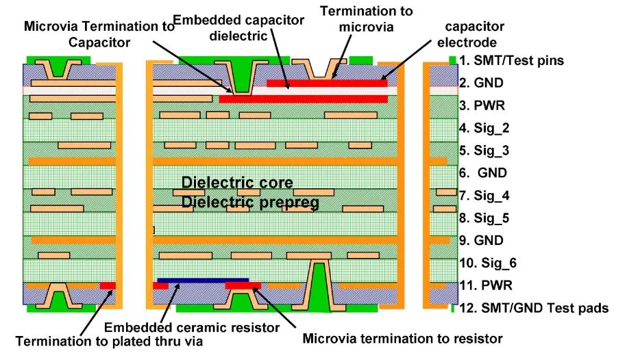
One primary hurdle is material behavior under processing stresses. Halogen-free resins absorb more moisture, elevating risks of popcorning and conductive anodic filamentation during preconditioning or assembly. Factories mitigate this through controlled storage humidity below 50 percent relative humidity and bake-out cycles before lamination. Warpage emerges from CTE mismatches between copper foils and dielectrics, exacerbated by asymmetric builds or uneven panel etching. Rigid laminates also accelerate drill wear, demanding optimized feed rates and peck drilling to maintain hole quality per IPC-6012E qualification specs.
Assembly introduces flux and solder paste compatibility issues. Halogen-free boards pair best with halide-free fluxes tested via oxygen bomb combustion methods, as standard ion chromatography misses covalently bound halogens. Reduced oxide removal in these fluxes impairs wetting on fine-pitch components, increasing head-in-pillow defects in BGA packages. Higher reflow temperatures strain profiles, potentially causing tombstoning on 0201 passives. Yield losses from these factors can add 5 to 10 percent to effective costs if not addressed early.
Practical Solutions for Halogen-Free PCB Manufacturing Cost Reduction
Strategic Material Selection
Selecting the right halogen-free laminates forms the foundation of cost control. Opt for phosphorus-nitrogen hybrids offering balanced Tg above 150 degrees Celsius and low Df under 0.005, avoiding over-specified high-end grades unless required for RF applications. Bulk qualification of two to three suppliers ensures competitive pricing and consistent lot performance. Factory data shows that standard HF FR-4 equivalents cut material premiums by focusing on volume-discounted grades. Pre-screen for drillability and etch resistance to sidestep secondary processing hikes.
Optimizing Halogen-Free PCB Design for Cost
Designers can slash expenses by prioritizing manufacturability from the outset. Symmetric stackups with balanced core and prepreg counts minimize warpage, reducing rework by aligning CTE across layers. Standardize board dimensions to fit common panel sizes, maximizing yield from 18 by 24 inch sheets and cutting scrap. Minimize via counts and layer transitions, as blind or buried vias inflate drilling costs on rigid materials. Incorporate wider traces where possible to ease etching and plating demands. These tweaks, rooted in DFM reviews, often yield 15 percent savings in prototype iterations.
Process Refinements in the Factory
Lamination cycles need tailoring for HF materials, with extended dwell times at 200 degrees Celsius to ensure void-free bonds without delamination. Increase press pressure slightly to compensate for higher filler content, per IPC-TM-650 adhesion tests. Drilling protocols shift to higher spindle speeds and shallower pecks, extending tool life despite material hardness. Plasma desmear replaces aggressive permanganate for better surface prep, curbing white ring defects. In assembly, precondition boards to J-STD-020E moisture sensitivity levels, using nitrogen reflow atmospheres to boost wetting uniformity.
Scaling and Supply Chain Tactics
Volume production unlocks economies, as fixed tooling amortizes over larger runs. Partner with fabricators experienced in HF flows, negotiating tiered pricing for panels exceeding 1000 units. Implement statistical process control for yield tracking, targeting above 95 percent first-pass rates through real-time SPC on warpage and peel strength. Recycle edge rails to offset material spends, aligning with sustainability ethos.
Conclusion
Achieving cost-effective halogen-free PCB manufacturing hinges on integrated strategies spanning materials, design, processes, and scale. By leveraging IPC standards for qualification and testing, factories deliver affordable halogen-free PCBs that meet performance demands. Key wins include symmetric designs reducing warpage, optimized drilling extending tool life, and volume commitments lowering per-unit costs. Engineers balancing cost comparison halogen vs non-halogen PCB will find these approaches bridge the gap effectively. Ultimately, halogen-free PCB manufacturing cost reduction empowers sustainable production without compromising reliability or compliance.
FAQs
Q1: How can engineers start reducing halogen-free PCB cost in early design stages?
A1: Focus on DFM by selecting standard HF laminates with proven drillability and symmetric stackups to cut warpage risks. Standardize panel utilization and minimize high-cost features like microvias. Prototype testing per IPC-TM-650 ensures process compatibility, avoiding expensive iterations. This factory-aligned method yields measurable savings in affordable halogen-free PCBs.
Q2: What is a typical cost comparison halogen vs non-halogen PCB?
A2: Halogen-free options incur 10 to 30 percent higher material costs due to alternative flame retardants, plus processing uplifts from drill wear. However, optimized designs and volumes narrow this to under 15 percent overall. Long-term benefits like compliance reduce total ownership costs. Factories emphasize bulk sourcing for parity.
Q3: What design tips optimize halogen-free PCB design for cost?
A3: Employ balanced layer counts and CTE-matched cores to prevent warpage, per standard qualification specs. Use larger panels and simpler routing to boost yields. Avoid exotic resins unless essential, sticking to mid-tier HF FR-4. These steps directly support halogen-free PCB manufacturing cost reduction while maintaining integrity.
Q4: Why do halogen-free PCBs sometimes warp more, and how to fix it?
A4: Higher moisture uptake and filler rigidity alter CTE, especially in asymmetric builds. Mitigate with symmetric stackups, controlled baking, and resin-rich interlayers. Measure via dial gauge post-lamination, targeting under 0.75 percent bow/twist. Process controls ensure reliable, cost-effective output.
References
IPC-4101B — Specification for Base Materials for Rigid and Multilayer Printed Boards. IPC, 2006
IPC-TM-650 — Test Methods Manual. IPC
IPC-6012E — Qualification and Performance Specification for Rigid Printed Boards. IPC, 2017
J-STD-020E — Moisture/Reflow Sensitivity Classification for Nonhermetic Surface Mount Devices. JEDEC/IPC, 2014