Introduction
Optimizing PCB layout for low-volume manufacturing demands a precise balance between functionality, reliability, and cost efficiency. In small-batch production, where quantities often range from prototypes to hundreds of units, design errors can lead to significant delays and expenses due to the lack of economies of scale. Effective PCB layout guidelines incorporate design for manufacturing (DFM) principles from the outset, minimizing revisions and ensuring high first-pass yields. Electric engineers must prioritize PCB design rules that align with fabrication and assembly capabilities, focusing on component placement and signal integrity to avoid common pitfalls. This approach not only streamlines production but also enhances overall board performance under real-world conditions. By adhering to structured strategies, designers can achieve excellence in low-volume runs, reducing risks associated with material handling and process variations.
Understanding Design for Manufacturing (DFM) in PCB Context
Design for manufacturing (DFM) refers to the systematic integration of manufacturability considerations into the PCB layout process to facilitate reliable production. For low-volume manufacturing, DFM becomes particularly vital because setup costs dominate, and iterative fixes are impractical. Core elements include defining clearances, trace widths, and via sizes that match standard fabrication tolerances, preventing defects like opens or shorts. Engineers apply DFM by simulating production constraints early, ensuring the layout supports automated optical inspection and soldering processes. This proactive methodology aligns design intent with shop floor realities, promoting consistency across small batches. Ultimately, robust DFM practices safeguard signal integrity while accommodating the flexibility required in prototype iterations.
Fundamental PCB Design Rules for Low-Volume Success
PCB design rules form the foundation of a manufacturable layout, specifying minimum dimensions for traces, spaces, pads, and holes to ensure process compatibility. In low-volume scenarios, adhering to conservative rules avoids custom tooling, which inflates costs. For instance, trace widths should account for current carrying capacity and etching variations, while annular rings around pads prevent drill breakout. Standard rules also dictate board outline clearances, recommending at least 5 mm from edges for mechanical stability during handling. Layer stackup decisions influence these rules, with symmetric builds reducing warpage in thin boards common to low-volume prototypes. Consistent application of these parameters streamlines quoting and fabrication, enabling faster turnaround.
IPC-2221 provides comprehensive guidelines for establishing these PCB design rules, covering aspects from conductor spacing to thermal management. Designers reference such standards to calibrate rulesets, ensuring compliance without overdesign.
Strategic Component Placement Guidelines
Component placement drives both assembly efficiency and electrical performance, making it a cornerstone of PCB layout guidelines for low-volume manufacturing. Engineers begin by grouping components by function, such as placing decoupling capacitors directly adjacent to power pins of integrated circuits to minimize loop inductance. Thermal management dictates separating high-power devices from sensitive analog sections, allowing adequate airflow and heat dissipation paths. Edge placement requires connectors and mounting hardware at least 5 mm from board borders to facilitate fixturing and prevent mechanical stress. Fine-pitch components benefit from staggered orientations to ease solder paste inspection, reducing bridging risks in vapor phase or selective soldering common to small runs. This logical arrangement optimizes trace lengths, preserves signal integrity, and supports test point accessibility.
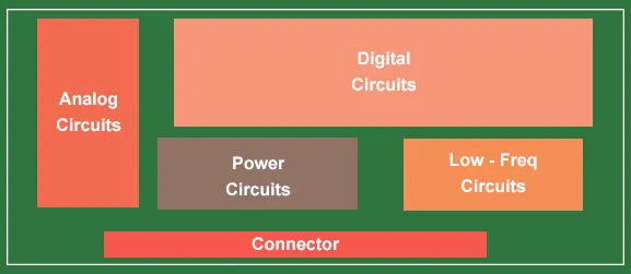
Prioritizing hierarchical placement, start with fixed elements like connectors, followed by ICs, passives, and finally electromechanical parts. Such sequencing minimizes rerouting disruptions and aligns with design for assembly flows.
Preserving Signal Integrity Through Layout Choices
Signal integrity in PCB layouts hinges on controlled impedance, minimal crosstalk, and matched propagation delays, especially critical in low-volume boards where debugging resources are limited. High-speed traces demand reference planes immediately adjacent, with ground pours filling unused areas to provide return paths. Length matching for differential pairs prevents skew, while avoiding 90-degree bends reduces reflections through chamfered corners. Via placement influences integrity, as stubs create discontinuities; blind or buried vias help in multilayer boards but increase complexity for low-volume. Engineers verify integrity by calculating characteristic impedance based on stackup dielectric constants and trace geometries. These practices ensure clean eye diagrams even in compact designs.
Routing Best Practices and Trace Management
Effective routing follows component placement, adhering to PCB design rules that prioritize short, direct paths for critical nets. Analog and digital signals route on dedicated layers to isolate noise, with power and ground planes providing low-impedance distribution. Minimize vias by using fanouts and jumpers judiciously, as each via adds capacitance and potential failure points in low-volume assembly. Clearance rules prevent arcing in high-voltage sections, typically 0.25 mm minimum between nets. Teardrops on pads enhance solder joint reliability, compensating for misalignment in reflow processes. Routing tools enforce these constraints, but manual review confirms manufacturability.

For low-volume, incorporate fiducials, at least three per panel, positioned asymmetrically for precise alignment during pick-and-place. Panelization rules, such as v-scoring or tab routing, enable efficient depanelization without stressing traces near edges.
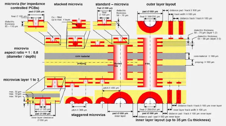
Advanced DFM Considerations: Vias, Clearances, and Tolerations
Vias represent potential weak points, so limit density and specify plating thickness per standards to withstand thermal cycling. Minimum drill sizes align with aspect ratios under 10:1 for reliable plating in small batches. Silkscreen and solder mask clearances, around 0.1 mm from pads, prevent bleed and ensure legibility for manual inspection. Tolerances for hole-to-pad alignment tighten for BGAs, but low-volume favors larger pitches to avoid X-ray needs. These elements collectively boost yield, as deviations amplify in non-high-volume lines.
IPC-A-600 outlines acceptability criteria for these features, guiding visual and automated checks post-fabrication.
Troubleshooting Layout Issues in Low-Volume Production
Common low-volume challenges include warpage from asymmetric stackups, addressed by balancing copper distribution and core selections. Solder bridging from tight component spacing resolves via stencil aperture reductions, though layout spacing prevents it upstream. Signal crosstalk in unrouted guards manifests as EMI failures; adding shielding vias mitigates this. Warped boards fail assembly; test setups measure bow and twist against class limits. Case in point: a prototype with uneven power plane splits caused 20% yield loss, fixed by redistributing pours and verifying in simulation. Iterative DFM reviews catch such issues pre-spin.
Conclusion
Mastering PCB layout for low-volume manufacturing requires integrating DFM, precise component placement, and signal integrity from schematic to gerber output. Adhering to established PCB design rules minimizes risks, accelerates production, and ensures reliable performance. Engineers benefit from structured approaches that prioritize manufacturability without compromising functionality. Low-volume success hinges on first-time-right designs, leveraging standards for consistency. Implementing these guidelines yields cost savings and faster market entry. Future layouts will evolve with materials, but core principles endure.
FAQs
Q1: What are the essential PCB layout guidelines for design for manufacturing (DFM) in low-volume runs?
A1: PCB layout guidelines for DFM emphasize minimum trace widths, pad clearances, and via annular rings to match fabrication capabilities. Component placement groups functions logically, with decoupling near ICs and edges cleared for handling. Fiducials and panelization support alignment and efficiency. Signal integrity rules include impedance control and plane references. These ensure high yields without custom processes.
Q2: How does component placement impact signal integrity and PCB design rules?
A2: Component placement directly affects signal integrity by influencing trace lengths and noise coupling. Place high-speed ICs centrally, with passives nearby to shorten loops. Follow PCB design rules for spacing to avoid crosstalk, maintaining at least 3H separation for parallel traces. Thermal grouping prevents hotspots degrading signals. Proper hierarchy reduces rerouting needs.
Q3: Why is signal integrity crucial in low-volume PCB manufacturing?
A3: Signal integrity prevents data errors in high-speed designs, vital for low-volume where respins are costly. Layout rules like length matching and ground stitching minimize reflections and EMI. Reference planes stabilize impedance, essential for compact boards. Verification early avoids assembly failures. DFM integration ensures these hold in production variations.
Q4: What PCB design rules should electric engineers follow for optimal DFM?
A4: Key PCB design rules include 0.15 mm minimum traces, 0.15 mm spaces, and 0.1 mm annular rings for standard processes. Stackups balance symmetry to curb warpage. Routing avoids acute angles, prioritizing critical nets first. J-STD-001 informs assembly criteria like solder fillet shapes. Conservative tolerances suit low-volume flexibility.
References
IPC-2221 — Generic Standard on Printed Board Design. IPC
IPC-A-600M — Acceptability of Printed Boards. IPC, 2025
J-STD-001 — Requirements for Soldered Electrical and Electronic Assemblies. IPC