Introduction
Plating processes form the backbone of printed circuit board manufacturing, ensuring reliable electrical connections and protection against environmental factors. In PCB production, copper plating on through-holes, vias, and surface features is essential for conductivity and signal integrity. Two primary methods dominate the industry: electroless plating and electrolytic plating. The electroless plating process relies on chemical reactions for deposition, while the electrolytic plating process uses electrical current to drive metal ions onto the board. Selecting the appropriate method depends on factors like board complexity, production volume, and performance requirements. This article compares these techniques to help electric engineers make informed decisions aligned with manufacturing standards.
Understanding the Electroless Plating Process
Electroless plating, also known as chemical or autocatalytic plating, deposits metal without an external electric current. The process begins with surface preparation, including cleaning and activation using palladium chloride to catalyze the reaction. A reducing agent in the plating bath, such as formaldehyde for copper, donates electrons to reduce metal ions from solution onto the substrate. This results in a uniform, thin layer of copper typically applied to non-conductive surfaces like dielectric materials in PCBs. The electroless plating process excels in initiating metallization on insulating boards, making it indispensable for through-hole plating in multilayer designs. Factory operations prioritize precise bath control to maintain deposit quality and avoid defects like voids or poor adhesion.
The process operates at moderate temperatures around 60 to 90 degrees Celsius, with pH levels carefully balanced to sustain the autocatalytic reaction. Unlike electrolytic methods, it covers complex geometries evenly, including high-aspect-ratio vias. However, bath stability demands regular replenishment of chemicals, influencing operational costs in high-volume production. Engineers value this method for its ability to seed panels before subsequent plating steps. Standards like IPC-6012E specify minimum thickness and uniformity requirements for such initial layers to ensure board reliability.
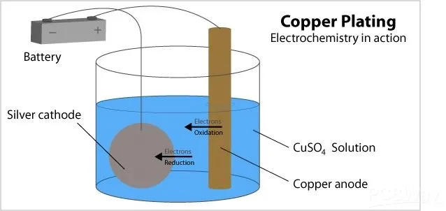
Exploring the Electrolytic Plating Process
Electrolytic plating, or electroplating, involves an electrochemical cell where the PCB acts as the cathode and a soluble anode provides metal ions. Direct current flows from an external power supply, reducing copper ions from an acidic sulfate bath onto the conductive surface. This method builds thicker deposits rapidly, ideal for achieving the bulk copper thickness needed for current-carrying traces and vias. The electrolytic plating process requires a pre-existing conductive layer, often from electroless plating, to initiate deposition. In practice, panels are racked, immersed in the bath, and plated under controlled current density to minimize irregularities. This technique dominates high-throughput factories due to its efficiency and scalability.
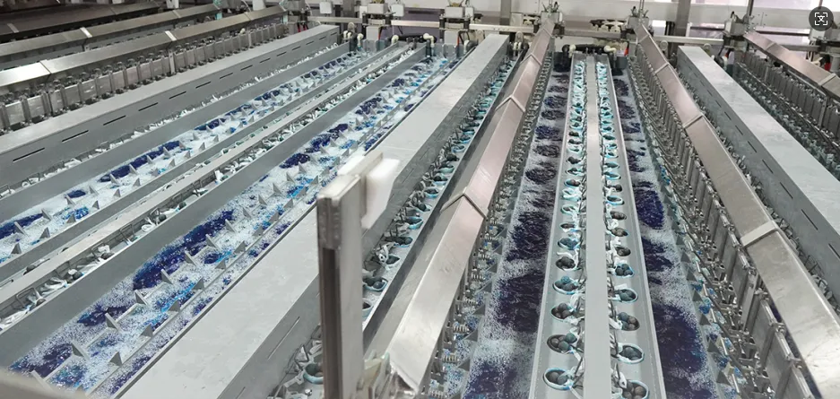
Bath composition includes copper sulfate, sulfuric acid, and additives for brightness and leveling. Current densities typically range from 10 to 30 ASF, allowing deposits up to 1 mil or more per hour. Edge effects and barrel plating variations pose challenges, requiring wing boards or pulse plating for uniformity. The process generates hydrogen gas at the cathode, necessitating good agitation and filtration. Compliance with IPC-A-600K ensures acceptability criteria for plating coverage and thickness across the board.
Key Technical Differences Between the Two Processes
The fundamental distinction lies in the driving force: chemical reduction in electroless plating versus electrical reduction in electrolytic plating. Electroless deposition occurs spontaneously on activated surfaces, producing conformal coatings without line-of-sight limitations. Electrolytic plating demands electrical conductivity, resulting in faster growth rates but potential non-uniformity on irregular shapes. Electroless layers are thinner, serving as seeds, while electrolytic builds the primary conductor mass. Waste generation differs too, with electroless baths producing more spent chemicals and electrolytic creating sludge from anodes. These differences impact factory layout, with electroless lines upstream of electrolytic tanks in typical workflows.
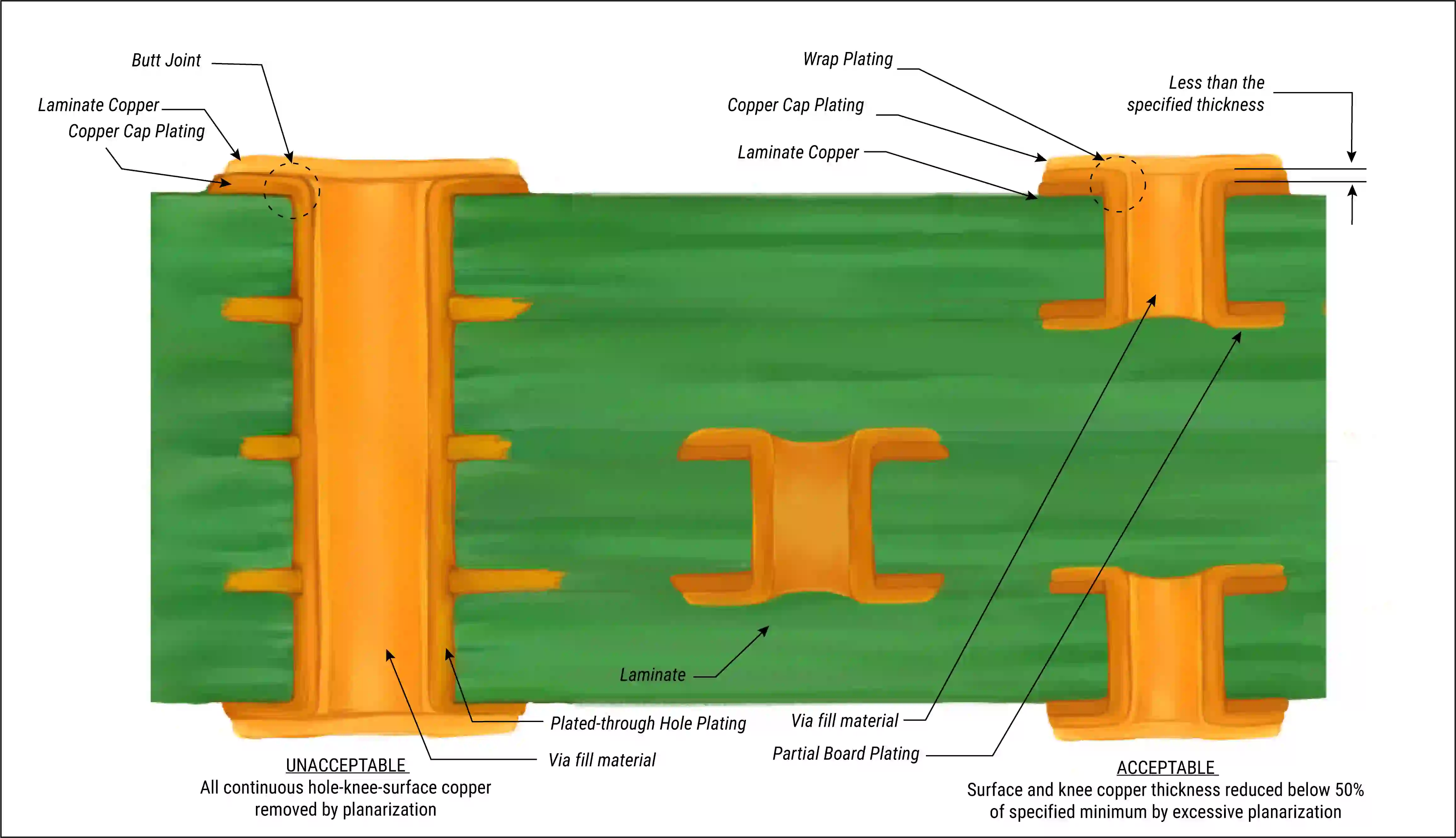
Process control varies significantly. Electroless baths degrade over time due to by-product buildup, requiring analysis via Hull cell tests or titration. Electrolytic systems monitor rectifier output and bath chemistry for consistent throwing power. Aspect ratio handling favors electroless for deep vias, as electrolytic suffers from dog-boning in high-ratio holes. Cost structures reflect this: electroless chemicals are pricier per panel, but electrolytic power and racking add expenses. Engineers must weigh these against design specs, such as via fill requirements per J-STD-003 for solderability preservation.
Electroless Plating Advantages and Electrolytic Plating Disadvantages
Electroless plating advantages include superior uniformity on non-planar surfaces, eliminating the need for electrical contacts during initial deposition. It enables plating of blind and buried vias in high-density interconnect boards without edge buildup. The process avoids mechanical wear from racking, reducing handling defects in fragile prototypes. Chemical deposition supports fine-line features down to 25 microns, critical for advanced nodes. Additionally, it operates without high currents, minimizing thermal stress on thin laminates.
Conversely, electrolytic plating disadvantages emerge in complex geometries, where current distribution leads to thinner deposits in recessed areas. Racking introduces point contacts that can cause dimples or skips, requiring post-treatment. High current densities risk burning or hydrogen embrittlement, compromising ductility. Waste management burdens factories with anode sludges and acid recovery systems. For low-volume runs, setup times for electrolytic lines inflate costs compared to batch electroless processing.
Applications of Electroless and Electrolytic Plating in PCBs
Electroless plating applications span initial metallization for all double-sided and multilayer boards, particularly in HDI designs with microvias. It suits prototyping and low-volume production where uniformity trumps speed. In RF and high-speed PCBs, the conformal seed layer supports precise pattern plating. Factories use it for ENIG (electroless nickel immersion gold) finishes, enhancing solderability and wire bondability. Its role extends to flex and rigid-flex circuits, where flexibility demands void-free coverage.
Electrolytic plating applications dominate panel and pattern plating for standard FR-4 boards in consumer electronics. High-volume automotive and telecom PCBs leverage its throughput for trace widths above 100 microns. Reel-to-reel electrolytic processes excel in flexible circuits, building robust conductors for power delivery. It fills through-holes completely in power supplies, ensuring low resistance paths. Hybrid flows, starting with electroless seed followed by electrolytic bulk, optimize most production scenarios.
Best Practices for Selecting and Implementing Plating Methods
Evaluate board design early: high-aspect ratios above 10:1 favor electroless initiation to avoid plating voids. For class 3 assemblies per IPC-6012E, combine methods for thickness exceeding 25 microns. Conduct design for manufacturability reviews to assess via geometry and panel size. In factories, maintain electroless bath life below 4 turnovers to prevent roughness. For electrolytic, use additives like carriers and levelers to improve throwing power beyond 70%. Pilot runs validate coverage with cross-section analysis, aligning with IPC-A-600K criteria.
Optimize costs by reserving electrolytic for high-volume panels and electroless for specialty features. Implement direct imaging before pattern plating to minimize undercuts. Monitor plating ductility via tensile tests, ensuring compliance with IPC standards for bend and thermal cycling. Sustainability practices include closed-loop electroless baths and electrolytic acid recycling. Engineers should collaborate with fabricators to specify plating sequence in Gerber files and stackups.
Conclusion
Electroless and electrolytic plating each offer unique strengths tailored to PCB manufacturing demands. The electroless plating process provides essential uniformity for seeding complex boards, while the electrolytic plating process delivers efficient thickness buildup for production-scale reliability. Understanding electroless plating advantages, electrolytic plating disadvantages, electroless plating applications, and electrolytic plating applications guides optimal selection. Factory-driven decisions, grounded in standards like IPC-6012E and IPC-A-600K, ensure performance without over-engineering. By matching method to design and volume, electric engineers achieve cost-effective, high-yield outcomes in diverse applications.
FAQs
Q1: What is the electroless plating process, and why is it used in PCB manufacturing?
A1: The electroless plating process involves chemical reduction to deposit a thin copper layer on non-conductive surfaces without electricity. It activates the board with palladium, then uses a reducing agent in a bath for uniform coverage. This method is crucial for initial metallization of through-holes and vias in multilayer PCBs. Factories rely on it for high-aspect-ratio features where electrolytic alone fails. It ensures reliable seeding before bulk plating, aligning with IPC standards for adhesion.
Q2: How does the electrolytic plating process differ from electroless in terms of speed and thickness?
A2: The electrolytic plating process uses electric current to rapidly deposit thick copper layers from an ion-rich bath. It achieves higher growth rates, building conductors for high-current paths efficiently. Unlike electroless, it requires prior conductivity and suits panel-level production. Thickness control via current density makes it ideal for standard boards, though uniformity challenges arise in complex shapes. This speed advantage drives its use in high-volume manufacturing.
Q3: What are the main electroless plating advantages for high-density PCBs?
A3: Electroless plating advantages include conformal deposition on irregular surfaces, perfect for microvias and fine features. It eliminates racking damage and supports HDI designs without dog-boning. Chemical uniformity aids signal integrity in high-speed applications. Factories appreciate its role in prototyping, reducing iterations. Combined with electrolytic, it meets IPC-A-600K for coverage in advanced nodes.
Q4: When should you choose electrolytic plating applications over electroless?
A4: Opt for electrolytic plating applications in high-volume, standard-thickness boards like power or automotive PCBs. It excels where speed and cost per panel matter, filling large vias completely. Use it post-electroless for bulk copper in FR-4 multilayers. Avoid for prototypes or ultra-fine lines due to non-uniformity risks. Standards guide minimum specs for reliable performance.
References
IPC-6012E - Qualification and Performance Specification for Rigid Printed Boards. IPC, 2017
IPC-A-600K - Acceptability of Printed Boards. IPC, 2020
J-STD-003B - Solderability Tests for Printed Boards, Components, and Solder. IPC, 2018


