Introduction
Multi-layer PTFE PCBs represent a significant advancement in printed circuit board technology, particularly for applications demanding high performance at elevated frequencies. Polytetrafluoroethylene (PTFE), with its low dielectric constant and minimal dissipation factor, forms the core material in these boards, enabling PTFE PCB multilayer designs that handle complex signal paths without degradation. Engineers designing RF systems, telecommunications equipment, or high-speed digital circuits increasingly turn to these boards for their ability to support PTFE PCB high density interconnects and precise routing. As designs grow more intricate, the inherent properties of PTFE address challenges like signal loss and crosstalk that plague traditional FR-4 materials. This exploration highlights how multi-layer configurations amplify these advantages, providing reliability in demanding environments. Understanding these benefits empowers electrical engineers to optimize their PCB layouts effectively.
What Are Multi-Layer PTFE PCBs and Why Do They Matter?
Multi-layer PTFE PCBs consist of multiple PTFE cores and prepregs stacked with copper foils, bonded under controlled pressure and temperature to form a rigid structure typically exceeding four layers. Unlike single or double-layer boards, these configurations allow for segregated power, ground, and signal planes, which is crucial for maintaining signal integrity in complex assemblies. The material's dielectric constant remains stable around 2.1 across a wide frequency range, far superior to epoxy-based laminates that exhibit higher variability. This stability directly supports PTFE PCB high density by permitting finer line widths and spaces, often down to 3 mils or less in advanced designs.
The relevance of PTFE PCB multilayer design stems from the escalating demands of modern electronics, where operating frequencies push beyond 10 GHz and data rates exceed 25 Gbps. Traditional materials suffer from increased insertion loss and phase shifts at these speeds, leading to bit errors and reduced system margins. PTFE mitigates these issues through its low loss tangent, typically under 0.0005 at microwave frequencies, ensuring signals propagate with minimal attenuation. For electrical engineers, this translates to fewer redesign iterations and higher yield rates during prototyping. Moreover, in aerospace and defense applications, the material's resistance to thermal cycling enhances long-term reliability.
Compliance with standards like IPC-6012 ensures these boards meet qualification criteria for rigid printed boards, including interlayer alignment and via integrity. As designs incorporate more components per square inch, the ability to route densely without compromising performance becomes paramount.
Technical Principles Behind Multi-Layer PTFE PCBs
The foundational advantage of PTFE lies in its dielectric properties, which enable low-impedance controlled routing essential for high-speed signals. In multi-layer stacks, PTFE prepregs provide uniform thickness control, typically between 0.005 to 0.020 inches per layer, allowing precise impedance matching across planes. This uniformity reduces variations in propagation delay, a critical factor in synchronous designs where skew must stay below picoseconds. Engineers leverage these properties in PTFE PCB routing by employing microstrip or stripline configurations, where the dielectric fully surrounds traces to minimize radiation losses.
Thermal management represents another key principle, as PTFE exhibits a low coefficient of thermal expansion (CTE) around 20-30 ppm/°C in the Z-axis, closely matching copper's 17 ppm/°C. This alignment prevents delamination during soldering or operational heating, a common failure mode in mismatched materials. In high-density layouts, where vias and blind/buried structures proliferate, this stability maintains electrical continuity. Furthermore, PTFE's high glass transition temperature above 260°C supports lead-free assembly processes without softening.
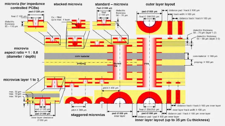
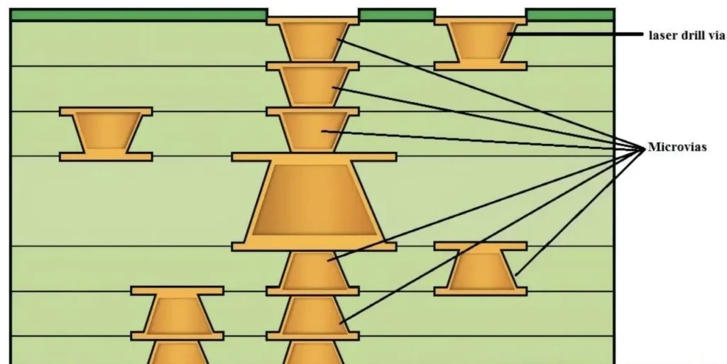
Mechanically, the material's low modulus requires careful handling during lamination, but results in boards with excellent dimensional stability post-fabrication. For PTFE PCB high density interconnects, sequential lamination techniques build layers incrementally, incorporating high-aspect-ratio vias that exceed 10:1 ratios reliably. These principles collectively enable complex topologies like HDI (high-density interconnect) features, where laser-drilled microvias connect multiple layers efficiently.
Signal integrity modeling reveals how PTFE's low dissipation factor preserves eye diagrams at high bit rates. Simulations show insertion loss under 0.5 dB/inch at 20 GHz, compared to over 1 dB for FR-4, directly impacting BER (bit error rate). Electrical engineers must account for these in stack-up design, balancing layer count with total board thickness, often capped at 0.062 inches for standard profiles.
Best Practices for PTFE PCB Multilayer Design and Routing
Effective PTFE PCB multilayer design begins with stack-up optimization, prioritizing symmetric builds to minimize warpage. Engineers should allocate inner layers for ground planes adjacent to signal layers, enhancing return path integrity and reducing EMI. Tooling holes and fiducials ensure registration accuracy within 0.003 inches, vital for aligning high-density features. Prepreg selection, with resin contents tuned for flow control, prevents voids during lamination cycles exceeding 350°C.
For PTFE PCB high density, adopt a via strategy combining through, blind, and buried types to shorten stub lengths and lower parasitics. Filled vias with conductive epoxy improve thermal dissipation in power planes, while back-drilling removes unused via stubs for gigahertz signals. Routing guidelines emphasize length-matched pairs for differential signals, with spacing exceeding 3x dielectric thickness to control crosstalk below -40 dB. Curved traces over straight lines reduce reflections in high-speed paths.
Fabrication tolerances tighten to ±0.001 inches for line widths in PTFE PCB routing, necessitating design rule checks early in the process. Sequential build-up processes, compliant with IPC standards, layer by layer photoimaging and plating, support feature sizes under 2 mils. Post-etch inspection verifies etch factor uniformity, preventing undercuts that degrade impedance.
Testing protocols include time-domain reflectometry (TDR) for impedance verification and vector network analysis (VNA) for S-parameter characterization. These confirm loss budgets align with system requirements before assembly. Engineers should also simulate thermal profiles, as PTFE's low thermal conductivity demands copper pours for heat spreading.
Challenges and Solutions in High-Density PTFE Implementations
While powerful, PTFE PCB multilayer design presents hurdles like higher moisture absorption during processing, necessitating bake-out cycles at 125°C for 24 hours. This step aligns with J-STD-033 guidelines for handling non-hermetic materials, preventing popcorning in reflow. Cost escalates with layer count, but yields justify it for volumes over 100 units.
Routing density amplifies crosstalk risks, addressed by ground stitching vias every 0.100 inches along trace perimeters. Mechanical drilling struggles with PTFE's abrasiveness, so laser ablation prevails for microvias, achieving taper angles under 15 degrees. Post-lamination planarization via oxide treatments enhances surface flatness for fine-line imaging.
Real-world insights from high-frequency prototypes show that iterative DFM (design for manufacturability) reviews cut respins by 30%. Collaboration between design and fab teams ensures aspect ratios stay viable, typically under 8:1 for plating uniformity.
Conclusion
Multi-layer PTFE PCBs offer unmatched benefits for complex designs, excelling in signal integrity, thermal stability, and high-density routing. PTFE PCB multilayer design facilitates intricate topologies with low loss and precise control, while PTFE PCB high density and routing capabilities meet the rigors of next-generation electronics. Electrical engineers gain a reliable platform for pushing frequency and data limits without compromise. By adhering to best practices and standards, these boards deliver performance that elevates system reliability. As designs evolve, PTFE remains a strategic choice for enduring high-stakes applications.
FAQs
Q1: What makes PTFE ideal for high-density multilayer designs?
A1: PTFE's low dielectric constant of approximately 2.1 and dissipation factor under 0.001 enable PTFE PCB high density by supporting fine-pitch traces and vias without excessive loss. In multilayer stacks, stable impedance control across layers minimizes skew in high-speed signals. Engineers achieve densities exceeding 1000 pins per square inch reliably. This suits RF and mmWave applications where traditional materials falter.
Q2: How does routing differ in PTFE PCB multilayer design?
A2: PTFE PCB routing prioritizes stripline configurations for full dielectric enclosure, reducing radiation compared to microstrips. Length tuning and differential pair spacing follow strict rules to maintain -40 dB crosstalk isolation. Laser-drilled vias enable dense fanouts, with back-drilling eliminating stubs for frequencies over 10 GHz. Logical stack-ups with ground planes adjacent to signals optimize return paths.
Q3: What are key considerations for thermal management in PTFE PCBs?
A3: PTFE's low CTE matching copper prevents warpage in multi-layer builds during thermal excursions up to 260°C. High-density areas require via stitching and copper fills for heat spreading, given the material's moderate conductivity. Compliance with IPC-6012 ensures via reliability under cycling. Simulations guide plane allocation to avoid hotspots in complex routing.
Q4: Can PTFE PCBs handle standard assembly processes?
A4: Yes, after proper bake-out per J-STD-033, PTFE boards withstand lead-free reflow profiles peaking at 260°C without delamination. Multilayer designs support BGA and fine-pitch components via precise via-in-pad features. Post-assembly testing verifies interlayer continuity, making them suitable for high-reliability sectors.
References
IPC-6012E - Qualification and Performance Specification for Rigid Printed Boards. IPC, 2017
IPC-A-600K - Acceptability of Printed Boards. IPC, 2020
J-STD-033D - Handling, Packing, Shipping, and Use of Moisture/Reflow Sensitive Surface Mount Devices. JEDEC/J-STD, 2021