Introduction
Efficient grounding forms the foundation of reliable PCB performance, especially in high-speed and mixed-signal designs. Poor grounding leads to issues like electromagnetic interference, signal distortion, and system instability, which can compromise overall functionality. Engineers must prioritize grounding strategies early in the design process to ensure low impedance return paths and minimal noise coupling between circuits. This article explores key techniques such as PCB ground planes, star grounding, multi-point grounding, methods for reducing noise, and shielding approaches. By understanding these elements, designers can create robust systems compliant with industry standards like IPC-2221B. Proper implementation not only enhances signal integrity but also simplifies electromagnetic compatibility testing.
Ground loops occur when multiple paths exist between grounds, inducing noise voltages proportional to the magnetic flux through the loop. This phenomenon is particularly problematic in analog-digital mixed boards, where digital switching noise couples into sensitive analog sections. Engineers evaluate grounding by considering frequency ranges: low-frequency signals favor isolated points, while high-speed signals demand distributed planes. The choice between techniques hinges on operating bandwidth and board complexity. Ultimately, efficient grounding supports thermal management by aiding heat dissipation through planes and reduces debugging time during prototyping.
The Fundamentals of PCB Grounding and Why It Matters
PCB grounding refers to the strategic connection of circuit components to a common reference potential, typically the chassis or earth ground, to provide stable voltage references and return currents. Ineffective grounding creates potential differences across the board, leading to ground bounce, crosstalk, and radiated emissions that violate regulatory limits. For electric engineers, mastering grounding is crucial because it directly impacts power distribution network integrity and high-frequency behavior. A well-designed system minimizes loop areas that act as antennas for electromagnetic interference. Industry relevance grows with denser boards and faster edge rates, where even small impedance mismatches amplify problems. Adhering to guidelines in IPC-2221B ensures designs achieve predictable performance across operating frequencies.
At its core, PCB grounding relies on minimizing the impedance of the return path for currents, as per fundamental circuit theory. Currents seek the lowest impedance path, so designers must provide wide, short conductors or planes to handle both DC and AC components. Skin effect at high frequencies confines currents to conductor surfaces, making plane thickness and proximity critical. PCB ground planes offer low inductance by spreading returns uniformly, unlike wire connections that concentrate fields. Impedance calculations guide layer allocation, with formulas deriving from transmission line models. These principles prevent voltage drops that degrade performance.
Core Technical Principles of Effective Grounding
Star grounding connects all circuits to a single point, ideal for low-frequency audio or DC systems where currents do not overlap significantly. This method avoids mutual coupling by ensuring separate return paths converge only at one node. However, at higher frequencies above a few MHz, parasitic inductances in spokes make it impractical due to increased impedance. Multi-point grounding, conversely, ties grounds together across the board via planes, suitable for RF and digital circuits where wavelength shortness justifies it. Transition frequency between methods typically falls around 1/(2*pi*L), where L is spoke inductance. Selecting the right approach requires simulating current distribution.
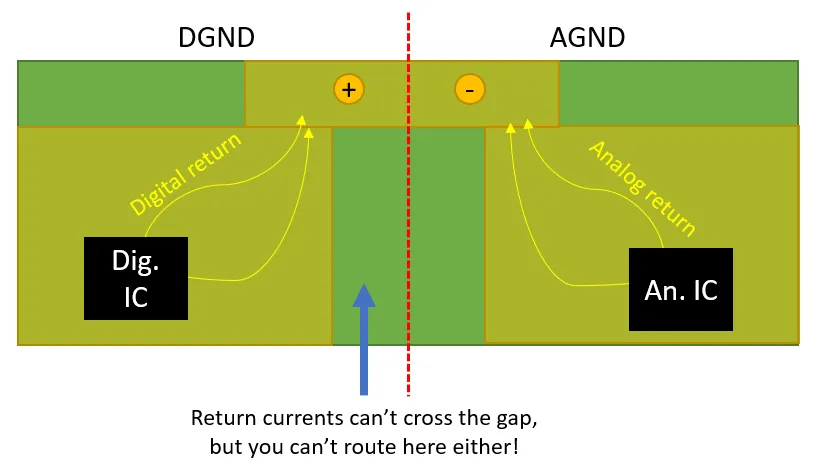
Noise reduction stems from partitioning the board into analog and digital ground regions, connected at a single quiet point to block digital noise. Split ground planes prevent high-frequency currents from spreading into sensitive areas, but careful bridging avoids floating sections. Via stitching along splits maintains plane integrity for shielding currents. Guard traces or moats further isolate sections by interrupting stray fields. These mechanisms rely on Faraday cage principles adapted to planar structures.
Leveraging PCB Ground Planes for Optimal Performance
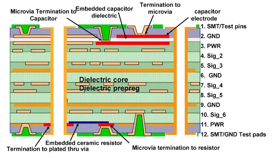
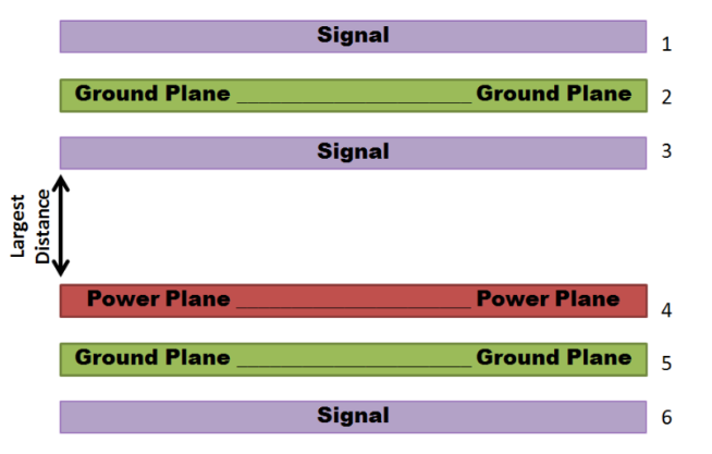
PCB ground planes serve as the backbone of modern multilayer boards, providing a low-impedance reference spanning the entire layer. A solid copper pour minimizes inductance to under 0.1 nH per square, far superior to traces, enabling effective multi-point grounding at GHz speeds. Placement on inner layers shields signals from external interference while offering thermal relief. Hatched planes reduce mechanical stress in high-power designs but slightly increase impedance. Engineers stack planes symmetrically around signal layers for balanced fields. Compliance with IPC-6012E ensures plane quality through lamination and plating specs.
To maximize effectiveness, flood pours avoiding cutouts near high-current paths, using power planes as complements. Multiple ground planes in stackups distribute return currents, reducing loop inductance by factors of 10 or more. Via fences stitch planes together, forming a continuous shield against EMI. For flexible boards, ground meshes adapt to bending without cracking. Simulation verifies plane resonance modes stay outside the bandwidth.
Strategies for Reducing Noise Through Grounding
Reducing noise begins with decoupling capacitors placed close to IC power pins, shunting high-frequency returns to ground planes. Values range from 0.1 uF ceramics for local bypass to bulk electrolytics for low frequencies, forming a broadband filter. Ground bounce from simultaneous switching diminishes with plane capacitance, typically 1 pF/cm2. Partitioning isolates noisy digital from precision analog, using single-point ties. Ferrite beads on boundaries attenuate common-mode noise without blocking returns.
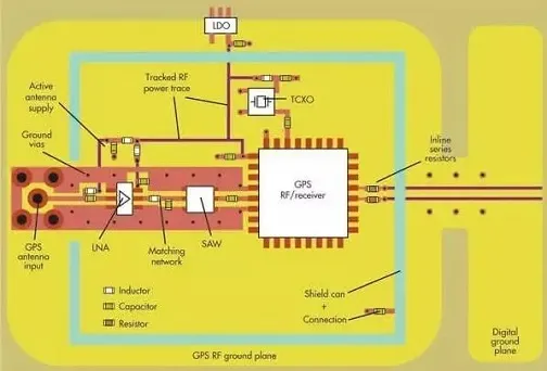
Shielding integrates with grounding via grounded enclosures or PCB-level guards. Enclose sensitive circuits in metal cans tied to ground planes, ensuring 360-degree contact. On-board shielding uses fenced traces or buried planes to contain fields. For RF modules, cavity shielding employs poured walls. These reduce radiated emissions by 20-40 dB, depending on enclosure integrity.
Best Practices for Designing an Efficient Grounding System
Start with stackup planning, allocating at least two ground planes in eight-layer boards for symmetry. Route signals over continuous grounds, avoiding splits under traces to prevent impedance discontinuities. Use dense via grids, spaced at lambda/20, for stitching. Simulate PDN impedance targeting under 10 mOhm up to Nyquist frequency. Fabricate with controlled impedance processes per IPC-6012E.
Test prototypes with near-field probes to map noise hotspots, iterating on plane fills. For mixed-signal, employ single-point bridges with 0 Ohm resistors for DC tie and AC block. Document grounding in schematics with plane symbols. Review for loop areas under 1 cm2.
Troubleshooting Common Grounding Issues
Ground loops manifest as 50/60 Hz hum, resolved by isolating power supplies or using differential signaling. High-frequency noise spikes indicate insufficient decoupling; add arrays near clocks. EMI failures from board edges suggest incomplete shielding, fixed by perimeter stitching. Simulate before fab to catch resonances. Oscilloscope eye diagrams reveal ground bounce, mitigated by plane proximity.
Conclusion
Designing an efficient PCB grounding system demands a holistic approach integrating PCB ground planes, star grounding, multi-point grounding, noise reduction, and shielding. Logical selection based on frequency and circuit type ensures low impedance and isolation. Adhering to standards like IPC-2221B and IPC-6012E guarantees manufacturability and performance. Engineers benefit from simulations and iterative testing to refine implementations. Ultimately, these practices yield reliable, compliant boards ready for production.
FAQs
Q1: What are PCB ground planes, and why are they essential for reducing noise?
A1: PCB ground planes are continuous copper layers providing low-impedance return paths and shielding. They distribute currents evenly, minimizing inductance and voltage drops that cause noise. In high-speed designs, planes offer inherent capacitance for decoupling, reducing ground bounce. Proper use aligns with multi-point grounding for frequencies above 1 MHz. This foundation supports signal integrity across the board.
Q2: How does star grounding differ from multi-point grounding in PCB designs?
A2: Star grounding converges all returns to one point, suiting low-frequency circuits to avoid coupling. Multi-point grounding connects via planes for high-speed applications, leveraging low plane impedance. Transition occurs around the frequency where spoke inductance exceeds plane benefits. Choose based on bandwidth to optimize noise reduction. Simulations confirm the best fit.
Q3: What role does shielding play in an efficient PCB grounding system?
A3: Shielding contains electromagnetic fields using grounded enclosures or on-board structures tied to ground planes. It blocks external interference and prevents emissions from internal sources. Combined with PCB ground planes, it enhances isolation in dense layouts. Vias and guards form effective barriers. This integral technique boosts overall system reliability.
Q4: When should engineers use split ground planes for noise reduction?
A4: Split ground planes partition analog and digital sections, connected at one point to block noise propagation. Ideal for mixed-signal boards with disparate requirements. Stitching vias maintain shield currents while isolating domains. Avoid under signals to prevent mode conversion. This practice ensures clean references per design standards.
References
IPC-2221B — Generic Standard on Printed Board Design. IPC, 2012
IPC-6012E — Qualification and Performance Specification for Rigid Printed Boards. IPC, 2017
IPC-A-600K — Acceptability of Printed Boards. IPC, 2020